eGaN FETs Are Low EMI Solutions!


GaN FETs can switch significantly faster than Si MOSFETs causing many system designers to ask − how does higher switching speeds impact EMI?
In this blog, EPC discusses simple mitigation techniques for consideration when designing switching converter systems using eGaN® FETs and will show why GaN FETs generate less EMI than MOSFETs, despite their fast-switching speeds.
Overview of an EMI System

Figure 1: Overview of an EMI system
Figure 1 shows the components of an EMI system:
The first component of an EMI system is the energy source, which can originate in various forms, for example as a switching event of a transistor. Energy from the source needs a transmission path such as conductors on a PCB. These transmission paths can form plates of a capacitor where the voltage can radiate as an E-field or in loops where the current path can radiate as an H-field. It is further possible for a loop to radiate an E-field and, vice versa, for the capacitor plates to radiate H-fields.
Regardless of transmission means and path, the EMI energy must be received. In the case of direct transmission, it is termed ‘conducted EMI’, and in the case of fields it is termed ‘radiation’.
The final component in an EMI system is the receiver which, by definition, is a circuit that becomes corrupted and results in undesirable behavior. The receiver circuit can be the same circuit that includes the source or a 3rd party circuit, for example, a radio receiver. In the case of 3rd party receiver circuits, the prevention of EMI-induced undesirable behavior is governed by EMI standards.
Addressing EMI mitigation measures for compliance and corruption prevention inevitably adds cost to a system. The closer to (and including) the source that steps are taken to address EMI, the lower the cost to the system.
The Effect of Layout
Layout is a zero-cost adder EMI mitigation measure. When designing converters, the layout inherently has parasitic inductance. In the synchronous buck converter example shown in figure 2, the effect of the loop inductance on the voltage overshoot of the switch-node following a rising edge hard-switching transition is shown.
The left image shows a layout with a loop inductance of approximately 1 nH and results in a 70% peak voltage overshoot with ringing. The right-side image shows a layout with a loop inductance of 400 pH and results in a 30% peak voltage overshoot with ringing.

Figure 2: Effect of layout on overshoot
The EMI generated is proportional to the square of the voltage overshoot magnitude and typically propagates as an E-field emanating from the conductors that form capacitors with ground. The loop inductance also conducts a current during the ringing period with corresponding EMI generated that is proportional to the square of the current magnitude, which typically propagates as an H-field emanating from the power loop circuit.
Reducing the power loop inductance by half reduces the EMI generated by a factor of four.
The Effect of Rise/Fall Time
Even though GaN FETs can switch much faster than MOSFETs, it is important to note that there is fundamentally no change in EMI energy simply because one device switches faster than another. There is only a shift in spectral content.
This is shown by example in figure 3 using a buck converter operating at 1 MHz, converting a 48 V input voltage to 12 V, for two switching transient conditions of 5 ns and 1 ns respectively. The graph shows the spectrum of the switch-node voltage for both transient conditions with the rising edge time set the same as the falling edge time and excludes voltage overshoot and ringing.
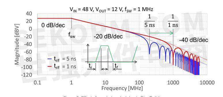
Figure 3: Effect of spectral contect due to Rise/Fall time
At 90 MHz, the spectral content has already been attenuated by 42 dB. In the 5 ns transient case, the first frequency of note is 200 MHz or 1 over 5 ns, and in the 1 ns transient case, the first frequency of note is 1 GHz or 1 over 1 ns.
The rate of decrease in spectral magnitude above these frequencies is 40 dB per decade, which means that filtering requirements are already very low, thus making it more critical to address the voltage overshoot ringing discussed earlier.
The switch-node effectively forms the plate of a capacitor with the ground being the second plate, making this form of EMI E-field radiant dominant.
The Effect of Reverse Recovery (QRR)
Lastly, as an example, the often-overlooked impact of reverse recovery on EMI using a hard-switching buck converter is evaluated.
Reverse recovery manifests as a shoot-through current in the power loop and, as was discussed earlier, a current in the power loop leads to voltage overshoot and ringing. The reverse recovery adds to the energy in the power loop and, thus, adds energy to the EMI noise source that is proportional to the square of the reverse recovery current. This reverse recovery current can be several times higher in magnitude than the inductor current of the buck converter.
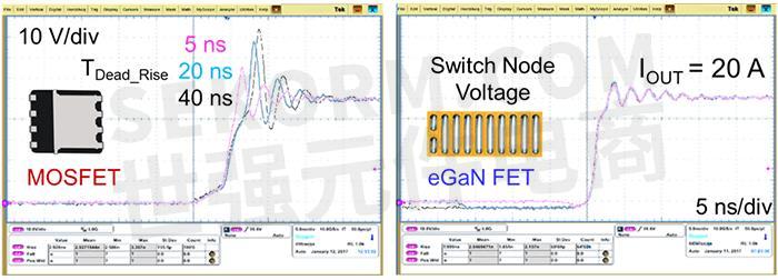
Figure 4: Effect of reverse recovery (QRR)
The left waveform of figure 4 shows the voltage overshoot and ringing for a MOSFET-based buck converter with dead times of 5 ns, 20 ns and 40 ns respectively, and the eGaN FET equivalent on the right waveform under the same operating conditions.
It can be seen on the right waveform that a change in dead time has no effect on the eGaN FET because it has zero reverse recovery.
Summary
eGaN FETs and ICs are EMI compatible. By adopting simple layout techniques, one can ensure significant reduction in EMI generation that adds zero cost to EMI mitigation.
The higher switching slew rates only result in a shift in spectral content but do not increase EMI energy. At higher frequencies, EMI reduction techniques are more effective resulting in lower cost to implement.
Finally, eGaN FETs and ICs come in wafer-level chip scale packages (WLCS) that have virtually zero internal inductance and, additionally have zero reverse recovery and, thus, inherently generate less EMI energy in hard-switching converters.
Despite their significantly faster switching speeds, eGaN FETs generate less EMI than MOSFETs.
- |
- +1 赞 0
- 收藏
- 评论 0
本文由翊翊所思转载自EPC,原文标题为:eGaN FETs Are Low EMI Solutions!,本站所有转载文章系出于传递更多信息之目的,且明确注明来源,不希望被转载的媒体或个人可与我们联系,我们将立即进行删除处理。
相关推荐

【产品】EPC新型200V eGaN FET的性能相比传统Si MOSFET提高了一倍
EPC推出新型200V eGaN FETs(氮化镓增强型功率晶体管),相比于传统的硅功率MOSFET的性能提高了一倍。新第五代设备的尺寸仅为上一代产品的一半,栅电极和源电极之间的距离有所减小,金属层的厚度增加等诸多改进使第五代FET的性能提高了一倍。

【产品】全新170V/6.8mΩ的eGaN FET EPC2059,尺寸仅2.8×1.4mm
EPC推出的EPC2059是一款增强型氮化镓功率晶体管(eGaN FET),漏源电压170V,典型导通电阻6.8mΩ,连续漏极电流24A,脉冲漏极电流102A,仅以带有焊条的钝化芯片形式提供,芯片尺寸2.8mm×1.4mm,无卤素。

EPC‘s New 200 V eGaN FETs Double The Performance Edge over The Aging Silicon Power MOSFET
Efficient Power Conversion (EPC) is doubling the performance distance between the aging silicon power MOSFET and eGaN transistors with 200V ratings.

【经验】EPC推出的用于氮化镓器件的LGA和BGA封装寄生电感低、尺寸小和热性能出色,应用时需考虑相关制造和设计事项
LGA和BGA封装提供了充分利用eGaN技术能力所必需的低寄生电感、小尺寸和出色的热性能。通过适当的制造技术,使用eGaN器件的组件将具有高产量和长而可靠的工作寿命。本文EPC将就LGA和BGA器件封装、正确的焊点大小和回流曲线等展开叙述,这些都是关键的设计考量因素。

成长中的氮化镓FET功率转换生态系统
描述- 本文介绍了基于eGaN®技术的功率转换系统,该系统相较于基于硅的替代品,具有更高的效率、更高的功率密度和更低的总体系统成本。文章详细阐述了eGaN FET生态系统,包括门驱动器、控制器和被动组件,并提供了相关产品的示例。此外,文章还讨论了eGaN FET在提高功率密度和效率方面的优势,以及如何选择合适的被动组件来优化性能。
型号- TEA1998TS,TEA1993TS,UP1966E,TEA1995T,MPQ1918,NCP81111,LM5113-Q1,EPC9165,NCP4306A,DSPIC33CK32MP102,TPS53632G,ISL8117A,LMG1210,NCP51820,FBS-GAM01P-C-PSE,FBS-GAM02P-C-PSE,FBS-GAM02-P-R50,LMG5200EVM-02,LTC7800,MIC2103/4,NCP4308A,UCD7138,TPS40400,EPC9078,SI8275GB-IM,LMG1205,SI8274GB1-IM,LM5140-Q1,EPC90120,ISL81807,ISL81806,NCP4305A,ISL70040SEH,MIC2127A

How2GaN | 如何设计具有最佳布局的eGaN® FET功率级
eGaN FET的开关速度比硅基MOSFET更快,因此需要更仔细地考虑印刷电路板(PCB)布局设计以最小化寄生电感。寄生电感会导致过冲电压更高,同时减慢开关速度。本篇笔记将会探讨使用eGaN FET设计最佳功率级布局的关键步骤,来避免上述不良影响并最大化转换器性能。

BRC Solar Selects EPC 100V eGaN FETs for Next Generation Solar Optimizer
Designing EPC‘s EPC2218 100V FETs into BRC Solar GmbH‘s next generation M500/14 power optimizer has enabled a higher current density due to the low power dissipation and the small size of the GaN FET making the critical load circuit more compact.

【应用】eGaN FET EPC2051助力激光雷达发射端高功率纳秒级别脉冲设计
在激光雷达的发射链路中,为实现雷达高分辨率的设计,需产生高功率、纳秒级别的激光脉冲。要达到这样的设计要求,普通MOS不能满足要求,需要采用GaN 搭配高功率Laser器件进行实现。EPC2051是EPC公司生产的氮化镓场效应晶体管(eGaN FET),已经成功的应用在激光雷达上。


【经验】EPC eGaN FET和eGaN IC PCB封装设计指南
一个良好的PCB封装设计对于GaN器件的一致性和可靠性是很重要的。本文是根据数据手册为EPC器件设计正确封装的指导原则——以EPC2016C和EPC2045为例,分别从LGA和BGA封装来完成介绍。

EAS egallium氮化物放大器2.1评估套件Class-D高性能egallium氮化物FET放大器平台
描述- 该资料介绍了EAS eGaNAMP 2.1评估套件,这是一款高性能的eGaN FET放大器平台。该平台包括eGaNAMP2016放大器模块、D2Audio DAE-3HT/DAE-6控制器/数字信号处理器,支持立体声、2.0和2.1通道音频配置。平台提供高保真音频参考,支持多种音频输入源接口,包括立体声模拟音频输入、光S/PDIF数字音频输入和AES-EBU数字音频输入。此外,该平台具有完全可编程的DSP前端,支持USB接口进行编程,并兼容D2Audio DAE-3、DAE-3HT和DAE-6 IC。

How to Design a 12V-to-60V Boost Converter with Low Temperature Rise Using eGaN FETs
This Talk EPC will examine the design of a 12V to 60V, 50W DC/DC power module with low temperature rise using eGaN FETs in the simple and low-cost synchronous boost topology.

电子商城


现货市场


服务
支持GSM / GPRS 等多种制式产品的射频测试,覆盖所有上行和下行的各项射频指标,包括频差、相差、调制、功率、功控、包络、邻道泄漏比、频谱、杂散、灵敏度、同道干扰、邻道干扰、互调、阻塞等等。满足CE / FCC / IC / TELEC等主流认证的射频测试需求。
实验室地址: 深圳 提交需求>
可烧录MCU/MPU,EPROM,EEPROM,FLASH,Nand Flash, PLD/CPLD,SD Card,TF Card, CF Card,eMMC Card,eMMC,MoviNand, OneNand等各类型IC,IC封装:DIP/SDIP/SOP/MSOP/QSOP/SSOP/TSOP/TSSOP/PLCC/QFP/QFN/MLP/MLF/BGA/CSP/SOT/DFN.
最小起订量: 1 提交需求>
授权代理品牌:集成电路


授权代理品牌:分立元件


授权代理品牌:接插件及结构件


授权代理品牌:部件、组件及配件


授权代理品牌:电源及模块


授权代理品牌:电子材料


授权代理品牌:仪器仪表及测试配组件


授权代理品牌:电工工具及材料


授权代理品牌:机械电子元件


授权代理品牌:加工与定制


登录 | 立即注册
提交评论