Power Up Your SPI Transfers


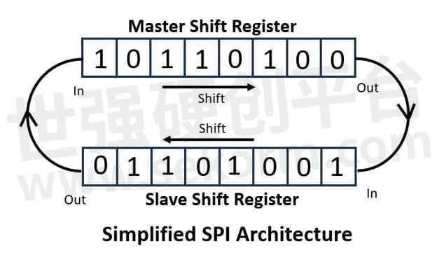
The Serial PeripheRAl Interface (SPI) has for many years been one of the simplest ways to interface external devices, such as sensors and external memories to a microcontroller. The SPI interface uses a simple synchronous serial protocol; this can be considered as a large serial buffer shared between two devices, a master and a slave, allowing data to be clocked between one device and the other under the control of a shift clock generated by the master device.

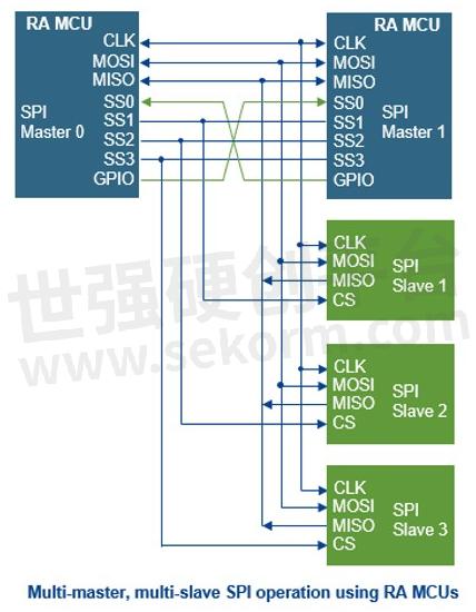
The SPI interface is controlled by the master device, which can connect to one or more slave devices using four logic signals. These are normally known as:
· SCLK: Serial Clock (clock signal generated by the Master)
· MOSI: Master Out Slave In (data output from Master)
· MISO: Master In Slave Out (data output from Slave)
· CS: Chip Select (active low signal generated by the Master to address individual devices and initiate the data transfer between them)
On the RA family of microcontrollers, SCLK is sometimes also known as the RSPCK, and the CS signal is known as the Slave Select Signal (SSL).
SPI is a non-standard standard, different implementations developed many years ago by semiconductor vendors such as Motorola and National Semiconductor have resulted in different naming conventions for these logic signals, depending on the device and the manufacturer. To complicate matters more, the different vendors developed SPI peripheral devices that can communicate in several different “flavors” of SPI which can complicate setting up communications between multiple devices.
Different slave devices may be designed to communicate by shifting data out during the rising or falling edge of the clock, either immediately when the CS becomes valid or on the next cycle, this is known as the clock polarity, and the data is sampled on the corresponding falling or rising edge, this is known as the clock phase.
Slave devices can come in any of these flavors so our SPI master must also be able to communicate in all the different flavors to be able to talk to every potential SPI slave device. In addition, SPI slave devices may expect to transfer data to either LSB or MSB first, with a selectable data length. With the use of multiple pins as Chip Selects, it’s possible to connect several different peripheral devices to one master and select each individually to initialize communications.

Using an SPI master on your microcontroller to interface your MCU to several SPI peripherals, all with different communication requirements, can become quite complex. This can greatly increase the size of the software driver required for the SPI interface and the need to support different flavors can also mean that you need to reconfigure the SPI interface between every data transfer you make to a different slave device.
The SPI interface on the RA family is quite a complex peripheral, as it must cope with the wide variety of different communications methods covered by SPI. The SPI interface can be programmed with a choice of clock polarity or clock phase, a programmable data transfer length selectable between 8 and 32 bits, a programmable bit rate, and the ability to directly control various SPI timings such as the delay before the Chip Select is released and the delay until next access. Full and half duplex, both transmit-only and receive-only operations are supported.
The RA SPI interface can automatically control up to four Chip Selects, allowing up to four devices to be handled automatically. Additional devices can be managed with software support using standard I/O pins. The SPI interface on the RA MCU also implements a selectable pin invert function.
The SPI interface on the RA has 128-bit transmit and receive buffers, which allow the use of up to four data frames transferable in one round of transmission or reception. These data frames are user selectable between one and four for each transfer.
A wide variety of errors can be detected by the SPI interface which can generate an interrupt; and, interrupts can also be generated on receive buffer full, transmit buffer empty, and transmission complete. These events can also be used to trigger a Data Transfer Controller (DTC) or Direct Memory Access (DMA) transfer.
Finally, the SPI interface can work in master mode or can be used in slave mode with an external master device.
An SPI transfer is triggered by the writing of data into the SPI data register. This register can be accessed on a byte, word, or longword basis and the SPI interface will automatically transfer the data into the transmit buffer and starts the serial transfer.
If you are communicating with multiple devices, perhaps using different flavors of SPI, with different baud rates, you need to set up the SPI interface each time and trigger the transfer, this can take up a lot of CPU overhead, so it would be much easier if we had a way to make this set up and the communications automatic.
The RENESAS Serial Peripheral Interface (RSPI) interface implemented on the RA 32-bit MCU family, provides an advanced command sequencer in the SPI logic to allow you to set up a series of automatic transfers between different SPI slave devices and to reconfigure the interface between each transfer. This can greatly reduce the requirements for the SPI interrupt service routine, as you no longer need to reconfigure the SPI interface between each transfer to a different device, and it can also speed up the transfer times for the same reason. Using the command sequencer to manage the SPI interface can also save power in your application, as your CPU can be asleep while the command sequencer automates the collection of data from different devices, using either the on-chip DMA controller or the DTC to fetch data from the on-chip SRAM to be sent or to load the received data into buffers in the SRAM to be analyzed later.
The SPI command sequencer allows a sequence of up to eight transfers to be executed in a looped sequence. After the sequence is completed, it will start again with the first command, you can see the available sequences below.
Sequence Length is 1 (n = 0→0→…)
Sequence Length is 2 (n = 0→1→0→…)
Sequence Length is 3 (n = 0→1→2→0→…)
Sequence Length is 4 (n = 0→1→2→3→0→…)
Sequence Length is 5 (n = 0→1→2→3→4→0→…)
Sequence Length is 6 (n = 0→1→2→3→4→5→0→…)
Sequence Length is 7 (n = 0→1→2→3→4→5→6→0→…)
Sequence Length is 8 (n =0→1→2→3→4→5→6→7→0→…)
For each command, you can set functions such as bit rate, clock polarity and phase, slave select logic level, data transfer length, and Most Significant Bit (MSB) or Least Significant Bit (LSB) first. For each command, you can also select which Chip Select pin to use for each command, so selecting a specific slave device, you can set how long after the transfer is complete the Chip Select signal is released, and you can set the access delay after the transfer before the start of the next transfer.

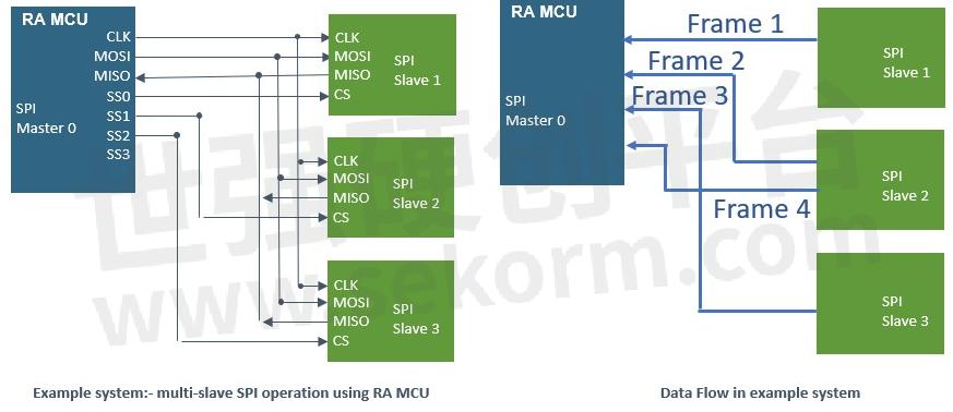
The diagram above shows an example system using SPI to connect the RA Master MCU to three slave devices. We can imagine such a system where the RA is collecting data regularly from several sensor devices, such as pressure, humidity, or temperature sensors. The command sequencer allows us to manage the collection of data from these sensors automatically with little CPU overhead. The command sequencer is used to manage the communications between these devices; in this example, we use a sequence length of four, as the sequence length is independent of the number of accesses to each slave device. In this sequence, we access Slave 2 twice, effectively at double the rate of the other two slave devices. Each data transfer between the master and slave has its own parameters, set up as part of the command structure.
The use of the command sequencer significantly reduces the CPU load to manage the reading of serial devices using the SPI interface, and when combined with the DTC or the DMA controller to automate the data transfer, this provides a powerful tool to manage data from external devices like sensors and memories completely automatically with minimum CPU intervention.
You can find out more about the SPI Interface implementation on RA microcontrollers and the SPI command sequencer in any of the RA device hardware manuals available for download from our website.
- |
- +1 赞 0
- 收藏
- 评论 0
本文由翊翊所思转载自RENESAS Blogs,原文标题为:Power Up Your SPI Transfers,本站所有转载文章系出于传递更多信息之目的,且明确注明来源,不希望被转载的媒体或个人可与我们联系,我们将立即进行删除处理。
相关推荐
【经验】瑞萨RA系列MCU时钟系统解析
本文以瑞萨MCU RA6T2为例,如下XTAL是外接的主时钟,频率为8到24M范围内任意可选。连接到单片机的XTAL和EXTAL引脚,HOCO:是片上高速振荡器,他不可以随意设置,比如RA6T2,他的HOCO为16,18,20M三选一。
【经验】基于瑞萨RH850/F1K的MCU 15833 CAN通信中断接收实现注意点
最近有客户在调试基于RH850/F1K的MCU CAN通信功能程序时,一直无法进入中断接收程序;经过查验总结问题所在点,步骤如下:1.在boot.asm文件,如果使用eiint作为表引用方法,启用下一行的宏。
【经验】瑞萨RA系列MCU使用模拟8080端口操作LCD显示屏
瑞萨RA系列MCU使用模拟8080端口操作LCD显示屏的方法和步骤。
RA2系列32位MCU
Renesas Electronics Corporation发布RA系列32位MCU,包括RA2、RA4、RA6等型号,基于ARM Cortex-M核心,提供高性能、高安全性和广泛连接性。RA系列MCU适用于工业自动化、建筑自动化、家用电器、计量、办公自动化和医疗保健等领域,具有低功耗、高集成度和灵活的软件包等特点。此外,RA系列MCU还提供丰富的开发工具和评估套件,以支持快速开发。
RENESAS - ARM®CORTEX®-M内核,FAST PROTOTYPING BOARDS,闪光,32-BIT MCU,单片机,快速原型板,32位微控制器,评估套件,ARM® CORTEX®-M CORES,FLASH,EVALUATION KITS,解决方案套件,MCU,SOLUTION KITS,FPB-RA2E2,R7FA2E1A9XXFM#AA0,R7FA2L1AB2DFP#AA0,R7FA2E1A53CFJ#AA0,FPB-RA2E1,RA2,R7FA2A1AB3CFJ#AA0,RSSK-RA2L1,R7FA2A1AB3CFJ,RA2 SERIES,RA2L1,R7FA2A1AB3CFM,RA2E1,RA2E2,EK-RA2L1,RA2A1,RA2A2,R7FA2E1A72DFM,EK-RA2E1,R7FA2E1A93CFL#AA0,EK-RA2E2,EK-RA2A1,RA FAMILY,ASI5 GATEWAY,电机控制,MOTOR CONTROL,MAGETIC ENCODER,VENDING MACHINE,电力,便携式音频设备,STEPPER MOTOR,SECURITY,INDUSTRIAL,窃贼探测,人机界面,AUTOMATED METER READING,低功耗,FIRE DETECTOR,不间断电源,UPS,BRUSHLESS DC MOTOR,OPTICAL ENCODER,WEARABLE DEVICE,ACCESS CONTROL,DOOR OPENER,流量计,VACUUM CLEANER,保健,能源,打印机,BUILDING AUTOMATION,感应电机,电容式触摸面板,TFT CONTROL,ASI5网关,FLEET TRACKING,监控系统,DATA CONCENTRATOR,INDUCTION MOTOR,通信网关,光编编码器,可穿戴设备,MONITORING SYSTEM,WHITE GOOD,网卡,BUILDING,HALL传感器,物联网应用,咖啡机,IO-LINK传感器,网关单元,IOT SENSING NODE,TOUCH INTERFACES,ELECTRICITY METER,物联网传感节点,IO-LINK网关,计量,触摸界面,IO-LINK SENSOR,OFFICE AUTOMATION,健康保健,IOT APPLICATIONS,医疗设备,POWER,楼宇自动化,防火面板,CAPACITIVE TOUCH PANEL,WIRED ETHERNET,磁编码器,智能家居类,FUNCTIONAL SAFETY,工业自动化,PANEL CONTROL,HEALTHCARE,自动售货机,WIRELESS,COMMUNICATION GATEWAY,医学,数据集中器,MOTION DETECTION,CLEANING ROBOT,门禁,PRINTER,ROBOTICS,FIRE PANEL,舰队追踪,AC DRIVES,PORTABLE AUDIO DEVICE,VOICE RECOGNITION,HVAC,交流伺服,STEPPER MOTOR,功率计,清洁类机器人,火灾探测器,METERING,白色货物,WEARABLE DEVICES,ENERGY,办公自动化,连接性,HEALTH CARE SOLUTIONS,语音识别,MEDICAL,AC SERVO,HALL SENSOR,CONSUMER ELECTRONICS,自动抄表,有线以太网,IO-LINK GATEWAY,HEALTH CARE,FLOW METER,SMART HOME,HOME APPLIANCE,COFFEE MACHINE,CONNECTIVITY,AIR CLEANER,SMOKE DETECTOR,COMMUNICATION,NETWORK CARD,运动检测,建筑物,安防,暖通空调,功能安全,BOILER CONTROL,通讯,消费电子,吸尘器,无线,DOOR OPENERS,LOW POWER,HEAT COST ALLOCATOR,TFT控制,工业,交流传动装置,机器人学,GATEWAY UNITS,锅炉控制,医疗保健解决方案,INDUSTRIAL AUTOMATION,HMI,BURGLAR DETECTION,热成本分配器,穿戴式设备,POWER METER,面板控制,MEDICAL EQUIPMENT,空气净化器,家用电器,烟雾探测器,ELECTRICITY METER,开门器,无刷直流电机
【经验】瑞萨RA系列MCU软件项目主控型号变更方法
在开发瑞萨(Renesas)的RA系列MCU的项目中,项目后期可能需要变更MCU型号,比如我们项目后期应用层软件代码增多,想要变更为更大存储的MCU型号,并且希望芯片管脚能够pin to pin,本文对此展开介绍。
32位MCU系列Renesas RA2E3集团
RA2E3系列是基于48 MHz Arm Cortex-M23核心的入门级超低功耗通用微控制器,提供32KB至64KB代码闪存、32或48引脚、5V电压选项。该系列与RA2E1系列兼容,适用于成本敏感型应用,支持丰富的模拟、无线、电机控制功能,以及低功耗模式,适用于物联网设备、工业自动化、传感器、消费电子等领域。
RENESAS - 入口线单片微控制器,ARM®CORTEX®-M23入门级超低功耗通用微控制器,ARM® CORTEX®-M23 ENTRY LEVEL ULTRA-LOW POWER GENERAL-PURPOSE MICROCONTROLLER,MCU,ENTRY LINE SINGLE-CHIP MICROCONTROLLER,单片机,RA FAMILY,RA2,RA4,R7FA2E3053CNE,R7FA2E3053CNH,RA6,R7FA2E3052DNE,RA8,R7FA2E3073CNE,RA2E3 GROUP,RA2E3,R7FA2E3053CFJ,R7FA2E3053CFL,R7FA2E3052DFJ,R7FA2E3073CNH,R7FA2E3052DFL,R7FA2E3072DNE,R7FA2E3072DNH,R7FA2E3073CFL,R7FA2E3072DFJ,R7FA2E3052DNH,R7FA2E3072DFL,R7FA2E3073CFJ,消费应用程序,MEDICAL DEVICES,HEALTHCARE DEVICES,医疗设备,楼宇自动化,IOT DEVICES,物联网设备,WEARABLE DEVICES,CONSUMER APPLICATIONS,HOME APPLIANCES,家用电器,医疗器件,工业用传感器,工业自动化,INDUSTRIAL AUTOMATION,INDUSTRIAL SENSORS,可穿戴设备,BUILDING AUTOMATION
【经验】以SPI为例子介绍瑞萨MCU RA2E1引脚配置
在configuration.xml文件下的PINS是RA2E1的引脚配置界面,在这里Ports的引脚和Peripherals的引脚是相互通用的,在Ports选中的引脚可以在Peripherals显示,在Peripherals选中的引脚可以在Ports中显示。
【经验】瑞萨RA系列MCU外部中断的配置和使用方法
和其他cortex内核的MCU相比,瑞萨的RA系列MCU,在中断的处理方法上是一样,当中断来临的时候,最先经过的的是IRQ(中断请求)寄存器,IRQ检测到中断的是时候,会向嵌套向量中断控制器NVIC发送中断信号。
32位MCU系列Renesas RA8D1系列
RENESAS - 基于ARM®CORTEX®-M85的图形微控制器,32位支持图形的MCU,32-BIT GRAPHICS-ENABLED MCUS,ARM® CORTEX®-M85 BASED GRAPHICS MICROCONTROLLER,MCU,单片机,R7FA8D1AHECBD,R7FA8D1BFECFC,R7FA8D1AFECFC,RA8D1,R7FA8D1BHECFC,R7FA8D1BHECBD,R7FA8D1AFECBD,R7FA8D1AHECFC,R7FA8D1BFECBD,RA8D1 GROUP,SECURITY CAMERAS,二维码阅读器,安全摄像头,图像分类,VIDEO DOORBELLS,恒温器,工业HMI,INDUSTRIAL HMI,PEOPLE DETECTION,机器视觉,患者健康监视器,MACHINE VISION,QR CODE READER,视频门铃,打印机显示,SECURITY PANELS,人员检测,PATIENT HEALTH MONITORS,安全面板,THERMOSTATS,PRINTER DISPLAYS,IMAGE CLASSIFICATION
【经验】瑞萨RA系列MCU通用SPI和SCI_SPI功能的区别
Renesas RA系列MCU中的SCI_SPI外设的驱动程序,该模块也实现了简单的SPI功能;通用的SPI外设的驱动程序,也实现了通用的SPI功能。本文主要介绍瑞萨RA系列通用SPI和SCI_SPI功能的区别,帮助大家快速的熟悉RA系列底层功能,快速的开发SPI外围器件产品。
【经验】瑞萨RA系列MCU PWM波形的设置方法
PWM波形在电机控制领域有广泛的应用,本文通过通俗易懂的图形界面操作方式,手把手的教会你如何使用瑞萨RA系列MCU的rgpt产生PWM波形。
瑞萨RA4E1集团32位MCU系列
Renesas RA4E1系列32位MCU采用Arm® Cortex®-M33核心,具备TrustZone安全功能,适用于入门级物联网应用。该系列具有平衡的低功耗和优化的功能集成,支持Flexible Software Package (FSP)生态系统。主要特点包括100MHz Cortex-M33核心、低至81µA/MHz的功耗、丰富的外设接口和多种封装选项。适用于智能家居、工业传感器、家庭娱乐等领域。
RENESAS - 32位微控制器,微控制器,EVALUATION KIT,评估套件,32-BIT MCU,MICROCONTROLLERS,RA4E1,RA4 SERIES,R7FA4E10D2CNE,R7FA4E10D2CFM,RA4,R7FA4E10B2CNE,R7FA4E10B2CFM,RA FAMILY,RA4E1 GROUP,RTK7FPA4E1S00001BE,SMART IOT AIR FILTER,INDUSTRIAL SENSOR HUB,HOME ENTERTAINMENT,SMART HOME,楼宇自动化,家庭娱乐,SMART COFFEE MACHINE,BUILDING AUTOMATION,语音命令,HOME APPLIANCES,内务MCU,智能家居类,家用电器,智能咖啡机,智能物联网空气过滤器,VOICE COMMAND,HOUSEKEEPING MCU,工业传感器集线器
Renesas Expands RA MCU Family with Two New Entry-Line Groups Offering Optimal Combination of Performance, Features and Value
Renesas announced the expansion of its 32-bit RA family of MCUs with two new Groups based on the Arm® Cortex®-M33 core with Arm TrustZone® technology. The new 100-MHz RA4E2 Group and 200-MHz RA6E2 Group are optimized to provide best-in-class power efficiency without compromising performance.
Renesas(瑞萨电子)RA2A1系列32位MCU数据手册
Renesas RA2A1 Group32-bit MCU Renesas Advanced (RA) Family Renesas RA2 Series
RENESAS - 32位MCU,32位微控制器,32-BIT MCU,RA2,R7FA2A1AB3CNF#AC0,R7FA2A1AB3CFJ#AA0,R7FA2A1AB3CFJ,R7FA2A1AB3CFM,R7FA2A1AB2CBT#AC0,R7FA2A1AB2CB,RA2A1,R7FA2A1AB3CNE#AC0,R7FA2A1AB3CFM#AA0,R7FA2A1AB2CBT,R7FA2A1AB3CNF,R7FA2A1AB3CNE,RA2 SERIES,32 KB SRAM,24位SIGMA-DELTA数模转换器(SDADC24),高达256 KB的代码闪存,SECURITY FEATURES,安全功能,12-BIT D/A CONVERTER (DAC12),16-BIT A/D CONVERTER (ADC16),12位模数转换器(DAC12),16位数模转换器(ADC16),24-BIT SIGMA-DELTA A/D CONVERTER (SDADC24),OPERATIONAL AMPLIFIER (OPAMP) WITH CONFIGURABLE SWITCHES,带可配置开关的运算放大器,32-KB SRAM,8位模数转换器(DAC8),8-BIT D/A CONVERTER (DAC8),UP TO 256-KB CODE FLASH MEMORY
32位MCU系列Renesas RA4M2集团
RENESAS - 32位微控制器,EVALUATION KIT,评估套件,32-BIT MCU,RA4M2 GROUP,RA4 SERIES,R7FA4M2AB3CN,RA4,R7FA4M2AD3CNE,R7FA4M2AC3CFP,RA4M2,R7FA4M2AC3CFL,R7FA4M2AC3CFM,RTK7EKA4M2S00001BE,R7FA4M2AD3CFM,R7FA4M2AD3CFL,R7FA4M2AB3CFP,R7FA4M2AD3CFP,R7FA4M2AB3CFM,R7FA4M2AC3CNE,R7FA4M2AB3CFL,SEWING MACHINES,暖通空调,AIR CONDITIONING,BOILER CONTROL,空调,加热,ROBOTICS,窃贼探测,IOT,INDUSTRY,DOOR OPENERS,火灾探测,HVAC,FIRE DETECTION,VENDING MACHINES,不间断电源,UPS,物联网,BURGLAR DETECTION,HEATING,PANEL CONTROL,工业,METERING,计量,增强的安全性,机器人学,缝纫机,锅炉控制,自动贩卖机,ELECTRICITY,ENHANCED SECURITY,面板控制,AUTOMATED METER READING,自动抄表,电,开门器
电子商城
现货市场
服务
可定制显示屏的尺寸0.96”~15.6”,分辨率80*160~3840*2160,TN/IPS视角,支持RGB、MCU、SPI、MIPI、LVDS、HDMI接口,配套定制玻璃、背光、FPCA/PCBA。
最小起订量: 1000 提交需求>
拥有IC烧录机20余款,100余台设备,可以烧录各种封装的IC;可烧录MCU、FLASH、EMMC、NAND FLASH、EPROM等各类型芯片,支持WIFI/BT模组PCBA烧录、测试。
最小起订量: 1 提交需求>


登录 | 立即注册
提交评论