How to Judge the Working State of MOS Tube?


How to judge the working state of the MOS tube
There are two working states of MOS tubes: enhanced and exhausted, divided into N channel and P channel.
The MOS tube is the metal, oxide, and semiconductor field effect transistor, or the metal-insulator and semiconductor. The source of the MOS tube and the drain can be switched, and they are both n-type areas formed in the P-TYPE Backgate. In most cases, the two regions are the same, and the switching of the two ends does not affect the performance of the device. Such devices are considered to be symmetrical.
How to judge the working status of MOS tube -N channel enhanced MOS field effect tube
1. Control the effect of VGS on ID and channel
①. VGS=0
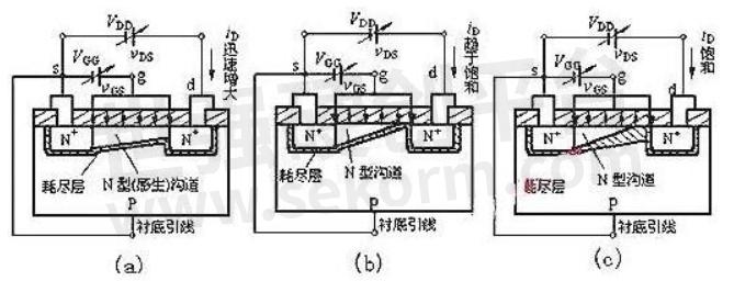
It can be seen from FIG. 1(a) that there are two PN junctions back-to-back between drain D and source S of the enhanced MOS tube. When the grid-source voltage VGS=0, even if the drain-source voltage VDS is added, and no matter what the polarity of VDS is, there is always a PN junction in the reversed state, and there is no conductive channel between the drain-source poles, so the drain current ID≈0 in this case.
②. VGS>0 situation
In the case of VGS > 0, an electric field is generated in the SiO2 insulation layer between the gate and substrate. An electric field is directed from the gate to the substrate perpendicular to the semiconductor surface. This electric field repels holes and attracts electrons.
Repulsive hole: The hole in the P-type substrate near the gate is repelled, leaving the immovable acceptor ion (negative ion), forming the depletion layer. Electron attraction: The attraction of electrons (electrons) from a P-TYPE substrate to the surface of the substrate.
2. Formation of conductive channel:
When the VGS value is small and the ability to attract electrons is not strong, there is still no conductive channel between leakage and source electrodes, as shown in FIG. 1(b). VGS increases, the increase in the number of electrons attracted to the substrate surface P, when the VGS reaches a certain value, the electrons in the grid near the substrate surface form a P N thin layer, and with two connected to the N + area, formed in the leak - source electrode N-type conductive channel, the conductive type, in contrast to the P substrate, so it is also called the inversion layer, as shown in figure 1 (c). The larger the VGS, the stronger the electric field on the semiconductor surface, the more electrons are attracted to the P substrate surface, the thicker the conductive channel, and the smaller the channel resistance.
The gate-source voltage at the beginning of the channel formation is called the open voltage and is denoted by VT.
The N-channel MOS tube discussed above cannot form a conductive channel when VGS < VT and the tube is in a cut-off state. Channel formation occurs only when VGS≥VT. This kind of MOS tube which must be at VGS≥VT to form a conductive channel is called an enhanced MOS tube. After the channel is formed, a drain current is generated by adding a positive voltage VDS between the drain and source electrodes.

The impact of VDS on ID
(1) Structure: The N-channel depletion MOS tube is basically similar to the N-channel enhancement MOS tube.
(2) Difference: When VGS=0 for the depletion MOS tube, a conductive channel exists between the leakage-source electrode, while the conductive channel appears only when VGS≥VT for the enhanced MOS tube.
(3) reasons: manufacturing n-channel depletion, MOS tubes are mixed with a large amount of alkali metal cations in SiO2 insulation Na + and K + (manufacturing P channel depletion MOS tube with negative ions), as shown in figure 1 (a), so even if VGS = 0, the effects of the electric field in the positive ion, leak - source electrode p-type substrate surface can also generate N channel induction (referred to as the initial channel), as long as plus forward voltage, VDS have current ids.
If positive VGS are added, the electric field between the gate and N channel will attract more electrons in the channel, the channel will be widened, the channel resistance will become smaller, and the ID will increase. On the contrary, when VGS is negative, the induced electrons in the channel decrease, the channel Narrows, the channel resistance increases, and the ID decreases. When VGS increases negatively to a certain value, the conductive channel disappears, ID tends to zero, and the pipe is cut off, so it is called the depletion type. The grid-source voltage when the channel disappears is called the clipping voltage, which is still expressed by VP. Similar to the N-channel junction fET, the clipping voltage VP of the N-channel depletion MOS tube is also negative, but the former can only work under the condition of VGS<0. And this is VGS=0, VGS>0.
Curve and current equation of N channel enhanced MOS tube

Output characteristic curve
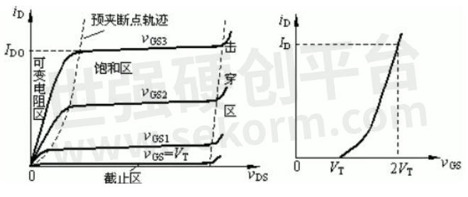
The output characteristic curve of the n-channel enhanced MOS tube is shown in Figure 1(a). Like junction ET, its output characteristic curve can be divided into variable resistance area, saturation area, cut-off area, and breakdown area. Transfer characteristic curve as shown in figure 1 (b), when used for amplification of the field effect tube device is working in a saturated zone (constant current), the ID hardly changes with VDS, namely different VDS of the transfer characteristic curve is almost overlap, so the available VDS is greater than a certain value (> VGS VDS - VT) after a transfer characteristic curve instead of the saturated zone all transfer characteristic curve.? The approximate relationship between ID and VGS.Similar to junction ET. In the saturation region, the approximate relationship between ID and VGS is:

In the equation, IDO is the drain current ID when VGS=2VT
P channel depletion MOS tube
P channel MOSFET works exactly the same as N channel MOSFET, except that the conductive carriers are different and the supply voltage polarity is different. This is similar to the bipolar transistor having NPN and PNP transistors.
- |
- +1 赞 0
- 收藏
- 评论 0
本文由荆菱雪转载自HI-SEMICON News,原文标题为:How to judge the working state of MOS tube,本站所有转载文章系出于传递更多信息之目的,且明确注明来源,不希望被转载的媒体或个人可与我们联系,我们将立即进行删除处理。
相关推荐
Miller Effect on MOS Tube Switches
The gate drive process of MOSFET can be simply understood as the charging and discharging process of the input capacitance (mainly CGS of the gate source capacitance) of the MOSFET. When THE CGS reaches the threshold voltage, MOSFET will enter the opening state.
MOS Tube Knowledge, Must Read!
According to the size of PCB board, select the appropriate PMOS tube size, in the case of limited on-board area, choose the small package as far as possible; As far as possible to select common packaging, to prepare for the subsequent selection of appropriate replacement material.
MOS tube structure principle
Structure and symbol (take n-channel enhanced type as an example) -- Two high-concentration N-type areas are diffused on a low-concentration P-type silicon as drain and source, the semiconductor surface is covered with a silicon dioxide insulation layer and an electrode is drawn as a gate.
MOS Switch Tube Selection and Principle Application
When the input voltage UI changes from high to low and the MOS tube changes from the on-off state to the cut-off state, the power UDD charges the stray capacitance CL via RD, charging time constant 1=RDCL, so the output voltage UO must pass a certain delay to change from the low level to the high level.
Switching Power Supply MOS Tube Loss
Switch Mode Power Supply, also known as switched Power Supply, switching converter, is a high-frequency Power conversion device, is a kind of Power Supply. Its function is to convert a potential voltage through different forms of architecture to the voltage or current required by the client. Switching power supplies convert voltages and currents between the inputs, which are mostly AC (such as mains power) or DC power, and the outputs, which are mostly devices requiring DC power, such as personal computers.
MOS Tube H Bridge Motor Drive Circuit Diagram
H bridge is a typical DC motor control circuit, because its circuit shape resembles the letter H, so it is named “H bridge“. Four audions constitute the four vertical legs of H, and the motor is the horizontal bar in H (note: the figure is only a schematic diagram, rather than a complete circuit diagram, in which the driving circuit of the audion is not drawn).
Details of MOS tube packaging
After the MOS tube chip is made, a shell is needed to be added to the MOS tube chip, which is the MOS tube package. The package housing mainly plays the role of support, protection and cooling, and also provides electrical connection and isolation for the chip, so as to form a complete circuit between MOS tube devices and other components. Different packaging, different design, MOS tube specifications, size, various electrical parameters, etc. will be different, and they can play a different role in the circuit will be different.
电子商城
服务
可根据用户的MOSFET管进行参数检测出具报告,静态参数最大电压:7500V、检测最大电流6000A;动态参数最大电压:3300V、检测最大电流:4500A。该测试标准满足GB、IEC及行业标准等,具备可靠性评估及老化实验能力。
实验室地址: 西安 提交需求>
定制液冷板尺寸5mm*5mm~3m*1.8m,厚度2mm-100mm,单相液冷板散热能力最高300W/cm²。
最小起订量: 1片 提交需求>


登录 | 立即注册
提交评论