How To Use An EPC Development Board to Evaluate The Performance of A Given GaN FET or IC in Common Applications?




EPC development boards offer the opportunity to evaluate eGaN® FETs and ICs in common applications. For example, the EPC9094 half-bridge development board can be configured as a buck or boost converter. The EPC9094 features the newly released EPC2054 200V 43mOhm max eGaN FET in a 1.3 x 1.3 mm 2 x 2 pin WLCSP package. The very low RDS(on) value of this very small FET permits it to support high current loads from a high voltage supply. To demonstrate this ability, EPC will modify the EPC9094 development board to a buck converter. Using a 140V supply, Spice simulation suggest 28V output at 2.5A will offer a high 90% efficiency. A Vishay IHLP-4040DZET330M11, 33μH, 4.4A, 95mOhm Max, 10.2 x 10.8 x 4mm inductor is selected which will provide 40% ripple at 500kHz. Output capacitors consisted of four 10uF Y5V 50V 1210 ceramic capacitors. The simulation showed a tradeoff between ripple current and overall efficiency when switching frequency was changed between 500kHz down to 375kHz. The simulation also showed that adjusting the dead time to permit full ZVS transition from high to low maximized the light load efficiency performance in the buck converter.
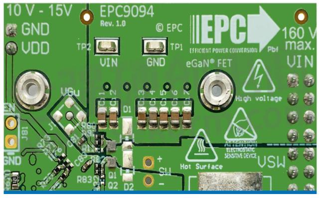
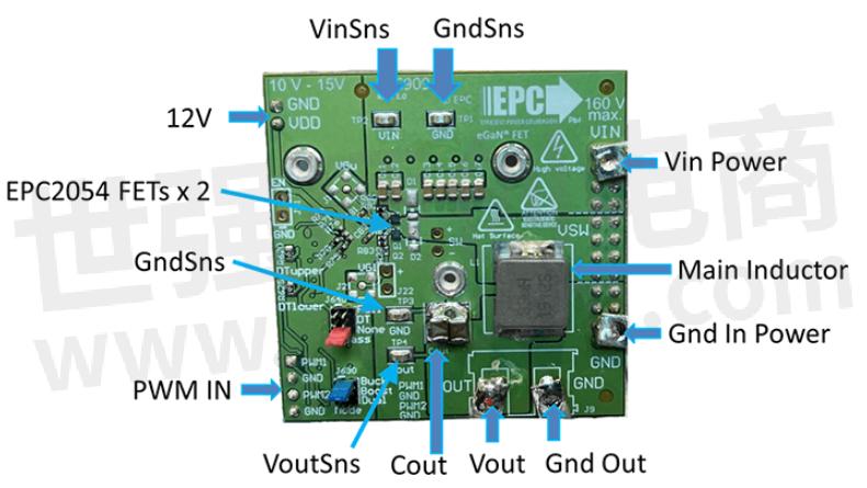
Figure 1: EPC9094 Development Board
Looking at the EPC9094 development board in Figure 1, there are multiple configuration options and connections. Power in is on the right and Power out is on the bottom. The board includes input voltage bulk capacitance. There is space to solder a large inductor and the output capacitors of your choice. Voltage sense points are offered for both input and output to permit high accuracy efficiency measurements. Additional pin-based connections are provided for gate driver bias power and PWM signal inputs. Finally, there are two jumpers offering three settings each. The blue jumper configures the board for Buck or Boost from a single PWM input or dual or independent high and low side FETs PWM inputs. The red jumper configures the dead time options.
1) No Bypass permits the development board's built-in dead time generators to function allowing customizable asymmetrical dead time for high and low side FETs.
2) DT Bypass means the development board's dead time circuit is deactivated.
3) Full Bypass reroutes both PWM input directly to the gate driver inputs with no signal processing delays.
The latter mode specially allows this development board to take advantage of the On-Semi's NCP51810/20 high voltage half bridge gate driver built in deadtime generator which is what we will use in this demonstration. Finally, there are three screw mounting studs of the correct height to allow for the optional attachment of a heatsink with TIM material to the top side of the EPC2054 FETs which would greatly extend the FET power handling range.
EPC's development boards do not come with traditional power terminals. However, banana jacks can easily be soldered to the terminals as shown in Figure 2. For the 12 V bias and the PWM pin input, hook clips can be used. BNC to hook clips adapters are available to make it easy to connect a pulse generator.
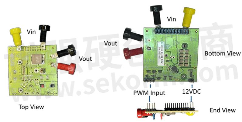
Figure 2: EPC9094 Connections
Figure 3 shows the switching waveform for the buck converter operating at full 2.5A load at 28V output. The OnSemi driver dead time was set to 40nS to allow full ZVS from high to low. The development board design demonstrates a peak 93.3% efficiency at full power with an operating temperature of 91°C. When the switching frequency was reduced to 375kHz, the efficiency improved to 94% with reduction in peak operating temperature down to 86.9°C as shown in the thermal image in Figure 5. Only the high side FET gets hot. A full table and plot of both 375 kHz and 500 kHz efficiency numbers are shown in Figure 4.
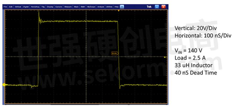
Figure 3:Switching waveform 140 VIN, 28 VOUT, 2.5 A
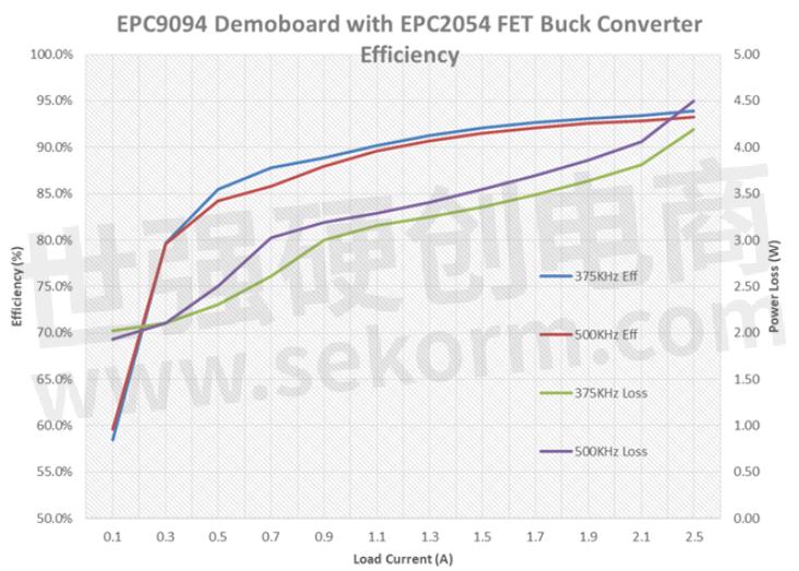
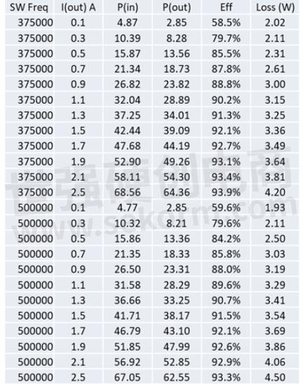
Figure 4: Efficiency and loss graph and table at 375kHz and 500kHz
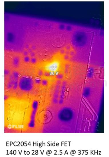
Figure 5: Thermal image of High Side FET
This article have shown that an EPC development board can easily be utilized to evaluate the performance of a given GaN FET or IC in common applications with very little setup effort. Configured the standard EPC9094 development board into a buck converter operating from 140VIN to 28VOUT at 2.5A to evaluate the performance of the 200V EPC2054 eGaN FET at various switching frequencies. With a set dead time of 40ns to allow full ZVS from high to low, the converter was able to demonstrate 94% efficiency at full power while switching at 375kHz.
- |
- +1 赞 0
- 收藏
- 评论 0
本文由董慧转载自EPC,原文标题为:From Development Board to Buck Converter,本站所有转载文章系出于传递更多信息之目的,且明确注明来源,不希望被转载的媒体或个人可与我们联系,我们将立即进行删除处理。
相关研发服务和供应服务
相关推荐
【经验】EPC eGaN FET和eGaN IC PCB封装设计指南
一个良好的PCB封装设计对于GaN器件的一致性和可靠性是很重要的。本文是根据数据手册为EPC器件设计正确封装的指导原则——以EPC2016C和EPC2045为例,分别从LGA和BGA封装来完成介绍。
How to Design a 12V-to-60V Boost Converter with Low Temperature Rise Using eGaN FETs
This Talk EPC will examine the design of a 12V to 60V, 50W DC/DC power module with low temperature rise using eGaN FETs in the simple and low-cost synchronous boost topology.
【经验】EPC分享eGaN FET如何缩小现代电源电路的物理尺寸——以LLC谐振转换器的设计为例
EPC设计的氮化镓场效应管具有小尺寸,高功率密度的特点,本文从LLC谐振转换器的设计说明了eGaN FET如何缩小现代电源电路的物理尺寸,并提高功率密度。
EPC eGaN®FET/晶体管选型表
EPC提供增强型氮化镓半桥功率晶体管/增强型功率晶体管/功率晶体管的选型:配置:Dual Common Source、Dual with Sync Boot、Half Bridge、Half Bridge Driver IC、HS FET + Driver + Level Shift、Single、Single - AEC Q101、Single – Rad Hard、Single with Gate Diode、Single with Gate Diode – AEC-Q101、Dual Common Source - AEC Q101,VDS最大值(V):15~350V;VGS最大值(V):5.75~7V
|
产品型号
|
品类
|
Configuration
|
VDSmax(V)
|
VGSmax(V)
|
Max RDS(on) (mΩ)
@ 5 VGS
|
QG typ(nC)
|
QGS typ (nC)
|
QGD typ (nC)
|
QOSS typ (nC)
|
QRR(nC)
|
CISS (pF)
|
COSS (pF)
|
CRSS (pF)
|
ID(A)
|
Pulsed ID (A)
|
Max TJ (°C)
|
Package(mm)
|
Launch Date
|
|
EPC2040
|
Enhancement Mode Power Transistor
|
Single
|
15
|
6
|
30
|
0.745
|
0.23
|
0.14
|
0.42
|
0
|
86
|
67
|
20
|
3.4
|
28
|
150
|
BGA 0.85 x 1.2
|
Apr, 2017
|
选型表 - EPC 立即选型
EPC(宜普)eGaN®FET与IC/开发板/演示板/评估套件选型指南
目录- eGaN FETs and Ics eGaN® Integrated Circuits Half-Bridge Development Boards DrGaN DC-DC Conversion Lidar/Motor Drive AC/DC Conversion
型号- EPC2212,EPC2214,EPC2059,EPC2216,EPC2215,EPC2218,EPC2016C,EPC2050,EPC9126,EPC2052,EPC2051,EPC2054,EPC2053,EPC2055,EPC9086,EPC2218A,EPC90153,EPC9087,EPC90154,EPC2069,EPC2102,EPC2101,EPC2104,EPC2103,EPC2106,EPC2105,EPC2107,EPC9018,EPC2065,EPC90151,EPC90152,EPC2067,EPC2100,EPC2221,EPC21701,EPC2066,EPC90150,EPC90145,EPC9097,EPC90142,EPC9098,EPC90143,EPC9099,EPC90148,EPC9092,EPC90149,EPC90146,EPC9094,EPC90147,EPC2219,EPC9091,EPC2619,EPC2036,EPC2035,EPC2038,EPC2037,EPC2014C,EPC2039,EPC9507,EPC2030,EPC2032,EPC9067,EPC2031,EPC9068,EPC2152,EPC2033,EPC9063,EPC9126HC,EPC9186,EPC8010,EPC9066,EPC2204A,EPC9061,EPC2308,EPC2307,EPC9005C,UP1966E,EPC2203,EPC9004C,EPC2202,EPC2204,EPC2015C,EPC2207,EPC2206,EPC2040,EPC2045,EPC2044,EPC9194,EPC2012C,EPC2019,EPC9049,EPC9203,EPC9204,EPC9205,EPC2252,EPC9166,EPC9167,EPC9047,EPC9201,EPC9041,EPC9162,EPC9165,EPC7020,EPC9160,EPC9040,EPC2024,EPC2302,EPC8009,EPC2001C,EPC2029,EPC2304,EPC2306,EPC2305,EPC8002,EPC2021,EPC9177,EPC2020,EPC9057,EPC9167HC,EPC2023,EPC9058,EPC9179,EPC2022,EPC8004,EPC9059,EPC9173,EPC9174,EPC9055,EPC9176,EPC9050,EPC9171,EPC9172,EPC2010C,EPC2034C,EPC7007,EPC7002,EPC9148,EPC2071,EPC7001,EPC23101,EPC23102,EPC23103,EPC90140,EPC9144,EPC23104,EPC2111,EPC7004,EPC2110,EPC7003,EPC90133,EPC90132,EPC9022,EPC90137,EPC90138,EPC90135,EPC90139,EPC7019,EPC7018,EPC9038,EPC9159,EPC2007C,EPC9039,EPC21603,EPC9156,EPC9036,EPC9157,EPC2088,EPC7014,EPC9037,EPC21601,EPC9158,EPC90122,EPC90123,EPC9031,EPC90120,EPC9153,EPC90121,EPC9033,EPC9154,EPC90124,EPC9150,EPC90128
BRC Solar Selects EPC 100V eGaN FETs for Next Generation Solar Optimizer
Designing EPC‘s EPC2218 100V FETs into BRC Solar GmbH‘s next generation M500/14 power optimizer has enabled a higher current density due to the low power dissipation and the small size of the GaN FET making the critical load circuit more compact.
【应用】eGaN FET EPC2051助力激光雷达发射端高功率纳秒级别脉冲设计
在激光雷达的发射链路中,为实现雷达高分辨率的设计,需产生高功率、纳秒级别的激光脉冲。要达到这样的设计要求,普通MOS不能满足要求,需要采用GaN 搭配高功率Laser器件进行实现。EPC2051是EPC公司生产的氮化镓场效应晶体管(eGaN FET),已经成功的应用在激光雷达上。
【产品】EPC新型200V eGaN FET的性能相比传统Si MOSFET提高了一倍
EPC推出新型200V eGaN FETs(氮化镓增强型功率晶体管),相比于传统的硅功率MOSFET的性能提高了一倍。新第五代设备的尺寸仅为上一代产品的一半,栅电极和源电极之间的距离有所减小,金属层的厚度增加等诸多改进使第五代FET的性能提高了一倍。
eGaN FETs Are Low EMI Solutions!
GaN FETs can switch significantly faster than Si MOSFETs causing many system designers to ask − how does higher switching speeds impact EMI? In this blog, EPC discusses simple mitigation techniques for consideration when designing switching converter systems using eGaN® FETs and will show why GaN FETs generate less EMI than MOSFETs, despite their fast-switching speeds.
【应用】如何使用200V eGaN FET设计2.5kW高效FCML图腾柱无桥PFC整流器
本文介绍了一种适用于数据中心应用的高效,高功率密度,2.5kW的基于eGaN FET的飞跨电容4电平图腾柱无桥整流器。采用EPC旗下200V/8mΩ的EPC2215用于高频支路,其转换器在900W至2.5kW的效率超过99%,在1.4kW时的峰值为99.25%。
【应用】采用eGaN FET EPC2045实现低成本高性能的DCDC设计
EPC2045是一款100V/7mΩ、电流能力高达16A的增强型氮化镓场效应晶体管。目前采用EPC2045的EPC9130的功率密度做到了1250W/in³,在成本上可以实现¥0.5/W以内的低成本设计。EPC2045相比于Si MOSFET,在损耗上优势也比较明显。在48V输入、12V/10A输出、驱动频率为500KHz的条件下,EPC2045可提供1.5%的更高效率。
电子商城
现货市场
服务
可烧录IC封装SOP/MSOP/SSOP/TSOP/TSSOP/PLCC/QFP/QFN/MLP/MLF/BGA/CSP/SOT/DFN;IC包装Tray/Tube/Tape;IC厂商不限,交期1-3天。支持IC测试(FT/SLT),管装、托盘装、卷带装包装转换,IC打印标记加工。
最小起订量: 1pcs 提交需求>
支持GSM / GPRS 等多种制式产品的射频测试,覆盖所有上行和下行的各项射频指标,包括频差、相差、调制、功率、功控、包络、邻道泄漏比、频谱、杂散、灵敏度、同道干扰、邻道干扰、互调、阻塞等等。满足CE / FCC / IC / TELEC等主流认证的射频测试需求。
实验室地址: 深圳 提交需求>





登录 | 立即注册
提交评论