Closing the Performance Gap Between DRAM and AI Processors


As the workhorse of semiconductor memory, DRAM holds a unique place in the industry thanks to its large storage capacity and ability to feed data and program code to the host processor quickly.
Lately, this unsung hero of the circuit board has been taking a backseat to its logic counterparts, as a wave of high-performance FPGAs, CPUs, GPUs, TPUs, and custom accelerator ASICs emerges to meet the massive data processing demands of predictive and generative AI applications. The sheer compute density of these rapidly emerging AI accelerators is shattering even the most ambitious expectations, and the number of processor cores inside data center servers continues to balloon.
However, such explosive growth has had consequences, given that advanced logic scaling continues to outpace DRAM scaling. This gap contributes to a widening performance mismatch between the two that threatens to compromise server performance by forcing high-speed (and costly) processors to waste compute cycles while waiting for main memory to catch up.
A New Approach to DRAM Interface Design
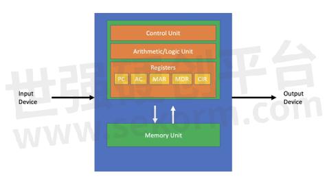
Of course, such imbalances are nothing new. The very nature of the classic Von Neumann model specifies the decoupling of the processor and memory, which creates a chokepoint that prevents designers from optimizing every compute cycle. With the industry’s design and manufacturing investment roadmaps more or less wedded to this architectural paradigm for the foreseeable future, RENESAS needs a new approach to bring processors and memory into closer alignment.

Figure 1 - Von Neumann Architecture
Indeed, DRAM designers are rushing to close the rift, most notably with the introduction of high-speed, high-capacity, third-generation DDR5 DRAM. But more must be done to mesh computing and memory. That was the motivation that drove Renesas to recently launch a registered clock driver (RCD) and client clock driver (CKD) for third-generation DDR5 DRAM servers and client systems across RENESAS entire portfolio of memory interfaces for dual inline memory modules (DIMMs), motherboards and embedded applications.
The new DDR5 RCD and DDR5 CKD ICs enable next-generation DIMMs with speeds of up to 6400 and 7200 mega transfers per second (MT/s), respectively, an increase from today’s 5600 MT/s transfer speeds. Renesas’ Gen 3 DDR5 RCD is designed for registered DIMMs (RDIMMs). The CKD is the first in the industry to interface with small-outline DIMMs (SODIMMs), unbuffered DIMMs (UDIMMs), high-performance gaming DIMMs, and memory-down applications for client platforms.

Figure 2 – DDR5 Server DIMM
Together, these new drivers enable a hierarchy of memories operating at different performance, power, and capacity levels. Their adoption is expected to drive the growth of so-called “chipsets,” an emerging form of heterogeneous computing that converges components with different functions, process nodes, and electrical characteristics. Heterogeneous computing is also driving research into new approaches to memory and logic within the device and module, inside the server, and across the entire server rack.
The Importance of Ecosystem Collaboration
RENESAS did not achieve this breakthrough in a vacuum. Working closely with the JEDEC standards body, Renesas is facilitating an ecosystem of development partners and serves as the glue that holds together DRAM and DIMM makers, CPU, GPU, and other logic providers, server designers – even hyperscale computing operators like Amazon, Google, and Microsoft. In addition to setting a shared roadmap and key performance indicators, the collective ensures design verification and interoperability testing at the device, module, and system level – and across all relevant software applications.
The imperative for close collaboration also led us to join the Compute Express Link™ (CXL™) Consortium. The consortium aims to develop open-source standards and technical specifications for data center interconnect. This includes a high-speed memory fabric that achieves performance parity with various forms of computing system architectures.
Ultimately, RENESAS' goal at Renesas is to empower device, module, and system architects to break conventional design constraints. Together, RENESAS can unleash the potential of a co-optimized compute-memory architecture and better meet the needs of increasingly sophisticated – and compute-intensive – AI applications.
- |
- +1 赞 0
- 收藏
- 评论 0
本文由翊翊所思转载自RENESAS Blogs,原文标题为:Closing the Performance Gap Between DRAM and AI Processors,本站所有转载文章系出于传递更多信息之目的,且明确注明来源,不希望被转载的媒体或个人可与我们联系,我们将立即进行删除处理。
相关推荐
What is Driving DDR5? & What does Renesas offer for DDR5?
Renesas‘ family of DDR5 and I³C expander ICs enables the next generation of server and client DIMM as well as server and client motherboard solutions to efficiently scale to superior performance, density and reliability while reducing overall system power.
【经验】反激式开关电源的RCD电路设计该如何选型?
本文将通过RCD电路中电阻电容和二极管参数的计算,然后完成元器件的选型,从而完成电路设计。TT系列电阻和京瓷系列电容及二极管可以出色的完成RCD电路的需求并保证电路的稳定运行。
非放电型RCD缓冲电路的设计
与放电型RCD缓冲电路不同,非放电型RCD缓冲电路的RSNB消耗的功率仅为浪涌能量,因此RSNB的容许损耗可以较小。这可以扩大RSNB的选择范围,使得能够增加CSNB的电容量,因而可以提高钳位的效果。
A Registering Clock Driver Used on DDR5 RDIMMs and LRDIMMs——Renesas RCD 5RCD0148HC2
The Renesas 5RCD0148HC2 (RCD) is a registering clock driver used on DDR5 RDIMMs and LRDIMMs. Its primary function is to buffer the Command Address (CA) bus, chip selects, and clock between the host controller and the DRAMs. It also creates a BCOM bus to control the data buffers for LRDIMMs.
瑞萨为高性能DDR5 DIMM开发提供一站式解决方案,给予卓越性能、密度和可靠性并降低整体系统功耗
与前几代DDR内存接口产品一样,瑞萨的器件处于市场领先地位。瑞萨拥有一个完整的IC系列来开发高性能的DDR5 DIMM,包括-RDIMM、LRDIMM、NVDIMM、UDIMM、SODIMM、游戏DIMM,以及用于服务器和客户端内存下降应用的内存接口产品。
DDR5寄存时钟驱动器7200 MT/s产品简介
描述- 该资料介绍了Rambus公司生产的DDR5 Registering Clock Driver (RCD) RCD4-GA0芯片,该芯片支持DDR5 Registered DIMMs (RDIMMs)以高达7200 MT/s的速度运行,适用于服务器等计算密集型数据中心应用。
【产品】用于DDR5内存模块的寄存时钟驱动器5RCD0148,支持速度高达4800MT/s
Renesas的5RCD0148HC2 (RCD) 是用于DDR5 RDIMM和LRDIMM的寄存时钟驱动器。它的主要功能是在主机控制器和 DRAM 之间缓冲命令地址 (CA) 总线、片选和时钟信号。它还产生了一个BCOM总线来控制LRDIMM的数据缓冲区。
DDR5寄存时钟驱动器5600 MT/s产品简介
描述- 该资料介绍了Rambus DDR5 Registering Clock Driver (RCD) 5600 MT/s芯片,该芯片支持DDR5 Registered DIMMs (RDIMMs)以高达5600 MT/s的速度运行,旨在为服务器提供突破性的内存带宽和容量,适用于计算密集型数据中心应用。
Renesas Introduces Industry‘s First Industrial Temperature Grade DDR5 and DDR4 Registered Clock Drivers
Renesas introduced the industry’s first industrial temperature DDR5 (5RCD0148H) and DDR4 (4RCD0232K) registered clock drivers (RCDs). The new devices are targeted at demanding applications.
Renesas Introduces Industry’s First Client Clock Driver and Gen 3 RCD to Enable Demanding DDR5 Client and Server DIMMs
The DDR5 RCD and DDR5 CKD ICs enable the next generation of DIMMs with speeds of up to 6400 and 7200 mega transfers per second (MT/s), respectively, an increase from today’s 5600 MT/s transfer speeds. Renesas’ Gen 3 DDR5 RCD is designed for registered DIMMs (RDIMMs).
【IC】瑞萨推出业界首款客户端时钟驱动器CKD和第3代RCD,支持严苛的DDR5客户端与服务器DIMMs应用
RENESAS宣布面向新兴的DDR5 DRAM服务器和客户端系统推出客户端时钟驱动器(CKD)和第三代DDR5寄存时钟驱动器(RCD),使下一代DIMM的速度分别达到每秒7200MT/s和6400MT/s,相比目前5600MT/s的传输速度均有所提升。
【产品】瑞萨电子新推出支持工业温度级DDR5和DDR4的寄存时钟驱动器,可带来2倍的通道速度提升
2021年11月4日,全球半导体解决方案供应商瑞萨电子集团今日宣布,推出支持工业温度等级DDR5(5RCD0148H)和DDR4(4RCD0232K)寄存时钟驱动器(RCD),面向要求严苛的边缘计算、汽车、工业4.0和5G等应用。
【产品】瑞萨电子率先推出面向下一代服务器、存储和通信系统应用的I3C智能开关,实现控制总线扩展
瑞萨电子推出面向下一代服务器主板和其它基础设施设备的I3C智能开关器件RG3MxxB12系列,极大提升了可扩展性和可靠性,同时降低高性能系统设计的复杂性,使具有多个发起设备控制器的I3C控制平面网络能够通过提高信号完整性和减少电容负载。
PA210009(R1):更改芯片厚度并为DDR5 RCD添加其他制造位置
描述- Renesas宣布对DDR5 RCD产品进行晶圆厚度变更,从8mil增加到10mil,以提高翘曲性能。内部认证已成功完成。同时,增加多个制造地点,以实现制造灵活性和最小化双重来源。变更对尺寸、形状、功能、质量和可靠性无影响。产品识别码截止日期为2021年12月20日以后。
型号- 5RCD0148HC3AVGI,5RCD0148HC3AVG,5RCD0148HC3AVG8,5RCD0148HC3AVGI8
电子商城
现货市场
服务
可定制单色LCD的尺寸:0.5”~15”;亮度:300~1600;视角:3“clock、6“clock、9“clock、12“clock、全视角。
最小起订量: 1000 提交需求>
可定制丙烯酸酯胶粘剂的粘度范围:250~36000 mPa·s,硬度范围:50Shore 00~85Shore D,其他参数如外观颜色,固化能量等也可按需定制。
最小起订量: 1 提交需求>


登录 | 立即注册
提交评论