What Is a DC/DC Converter? Part 3


Introduction
Hello, everyone. In the previous volume, I mentioned that the energy stored in and released from an inductor, which is an element of the buck DC/DC Converters, is used for the operation of the Buck DC/DC converters. This time, I will explain that the function of energy stored in and released from the inductor realizes the boost operation which makes a higher output voltage than the input voltage, and the inverting operation which makes negative output voltage from the positive input voltage by just changing how the power supply, an inductor, and a switch are connected. I will also explain control methods other than time ratio control.
Contents
Voltage Generation by Cutting Off the Inductor Current
Image of Output Voltage Generation of Buck/Boost/Inverting DC/DC Converters
DC/DC Converters' Control Method
Conclusion
Voltage Generation by Cutting Off the Inductor Current
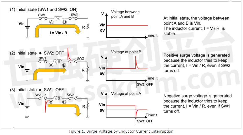
An easy circuit for explanation is shown in Figure 1. Consider the case that a constant current, I = Vin / R, flows through the inductor, and the inductor voltage between point A and point B is Vin as the initial state. In this situation, if SW2, between the inductor and resistor R, turns off, how does the voltage of point B change? Even if the SW2 turns off, the inductor tries to flow the current (I = Vin / R) continuously, the voltage of point B rises drastically, and a kind of surge voltage is generated in positive direction. Boost DC/DC converters control this operation to generate a stable voltage higher than the input voltage. On the other hand, from the initial state, if SW1, between the inductor and power supply Vin, turns off, how the voltage of point A change? Even if SW1 turns off, the inductor tries to flow the current (I = Vin / R) continuously, the voltage of point A goes down drastically, and a kind of surge voltage is generated with a negative voltage of less than 0V. Inverting DC/DC converters control this operation to generate a stable voltage lower than 0V.
Boost DC/DC Converters
In terms of boost DC/DC converters, Input power supply: Vin, Inductor L, SW1, SW2, Output capacitor Cout are connected as shown in Figure 2. According to Figure 2, the operation can be explained as follows:
Step 1: When SW1 turns on, the current from the power supply Vin flows through the inductor to the GND and gradually increases, and energy is stored in the inductor.
Step 2: When the SW1 turns off and SW2 turns on, the inductor current continues to flow. During this Step 2, the energy stored in the inductor is released.
With this current the output capacitor is charged with this current, and the output voltage rises. I hope you can imagine that the output voltage, Vout, rises by repeating Step 1 and Step 2.
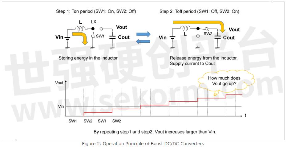
Then, by how much does the output voltage go up? The answer is shown in Figure 3.
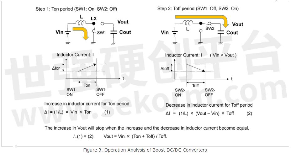
If voltage "V" is forced across an inductor with inductance "L" for the time period "T", then the amount in inductor current, ΔI, can be described by the formula below:
ΔI = (1 / L) × V × T
Step 1: SW1 turns on for the Ton period. The input voltage Vin is forced across the inductor for the Ton period. The increase in inductor current ΔIon can be calculated as shown in the next formula:
ΔIon = (1 / L) × Vin × Ton. ... (1)
Step 2: SW2 turns on for the Toff period. The voltage "Vout - Vin" is forced across the inductor for the Toff period. The decrease in inductor current ΔIoff can be calculated as shown in the next formula:
ΔIoff = (1 / L) × (Vout – Vin)× Toff. ... (2)
When the increase in inductor current, ΔIon, and the decrease in inductor current, ΔIoff, are equal, the increase in output voltage stops. Thus, by using equation (1) = (2), we obtain Vout as:
Vout = Vin × (Ton + Toff) / Toff.
As described above, the configuration is shown in Figure 2, and the voltage higher than Vin is generated by switching two switches at a certain time ratio. The output voltage is adjusted by the time ratio. I hope you now understand the operation of boost DC/DC converters.
Output Voltage Smoothing by Capacitor
Buck DC/DC converters supply a current to the output load during both the Ton and Toff periods. However, boost and inverting DC/DC converters do not supply a current to the output load during the Ton period.
In buck DC/DC converters, the filter is composed of an inductor and a capacitor, and the inductor also plays a "smoothing" role. However, in boost DC/DC converters, the inductor does not contribute to smoothing, and only the capacitor plays the role of smoothing. Therefore, a capacitor with a relatively large capacitance is required. The role of the inductor in boosting DC/DC converters is only "energy store and release."
Output Current of DC/DC Converters
Suppose that the average current from Vin is Iin, and the output current is Iout, then,
Vin × Iin = Vout × Iout
By this equation, the bigger the ratio of the output voltage against the input voltage, or boost ratio is, the lesser the maximum output current is.
* While Vin × Iin is supplied during the Ton period and the Toff period, current flows through the inductor to GND during the Ton period. Therefore, one might think that energy is consumed by the current consumed during this period, but energy is not consumed during the Ton period. This is the period during which energy equivalent to Vin × Iin is stored in the inductor.
Inverting DC/DC Converters
To compose an inverting DC/DC converter, input power supply: Vin, inductor: L, SW1, SW2, output capacitor: Cout is connected as shown in Figure 4. Based on Figure 4, the operation can be explained as follows:
Step 1: When SW1 turns on, the current from the power supply Vin flows through the inductor to the GND and gradually increases. At this time, energy is stored in the inductor by the current flowing through the inductor.
Step 2: When the SW1 turns off and SW2 turns on, the inductor current continues to flow. During this Step 2, the stored energy in the inductor is released as a current.
The output capacitor is discharged with this current, and the output voltage decreases. You can imagine that the output voltage, Vout, decreases below 0 V by alternately switching between Step 1 and Step 2.
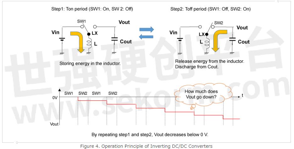
Then, how much does the output voltage go down? The answer is shown in Figure 5.
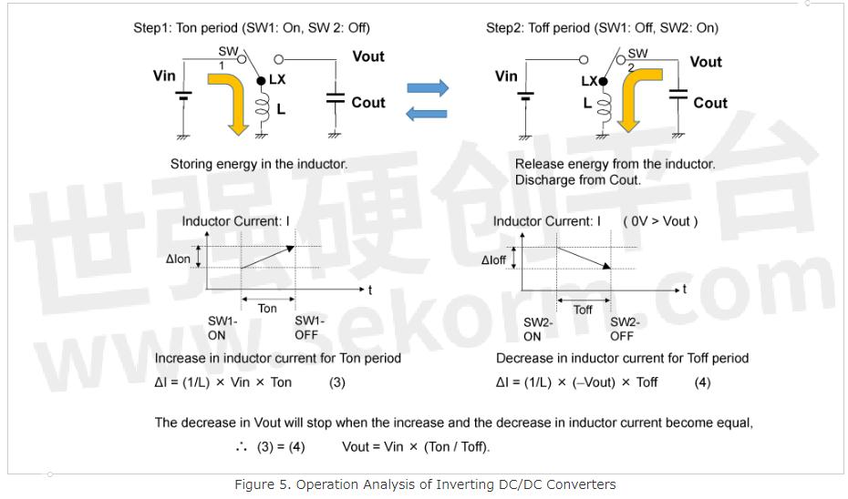
It is analyzed in the same way as boost DC/DC converters.
Step 1: SW1 turns on for the Ton period. The input voltage Vin is forced across the inductor for the Ton period. The increase in inductor current ΔIon can be calculated as shown in the next formula:
ΔIon = (1 / L) × Vin × Ton. ... (3)
Step 2: SW2 turns on for the Toff period. The voltage "|Vout|" is forced across the inductor for the Toff period. The decrease in inductor current ΔIoff can be calculated as shown in the next formula:
ΔIoff = (1 / L) × |Vout| × Toff. ... (4)
When the increase in inductor current, ΔIon, and the decrease in that, ΔIoff, are equal, the falling of the output voltage stops. Thus, by using equation (3) = (4), we obtain Vout as:
|Vout| = Vin × (Ton / Toff).
As described above, the configuration is shown in Figure 4, and the voltage below 0V is regulated by switching two switches at a certain time ratio. The output voltage is adjusted by the time ratio. I hope you now understand the operation of inverting DC/DC converters.
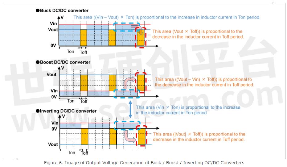
Image of Output Voltage Generation of Buck/Boost/Inverting DC/DC Converters
For each topology of DC/DC converters, when the increasing inductor current amount, ΔIon, and decreasing inductor current amount, ΔIoff are equal, suppose that the voltage between both edges of the inductor is Von during Ton, Voff during Toff, then the next formula is true.
Von × Ton = Voff × Toff
As shown in Figure 6, the image of the output voltage of the DC/DC converters can be easily described.
Buck DC/DC Converters
Vout during the Toff period is filled and averaged by (Vin − Vout) × Ton,
∴ Vout = Vin × Ton / (Ton + Toff).
Boost DC/DC Converters
Vin × Ton / Toff is added to Vin,
∴ Vout = Vin × (Ton + Toff) / Toff.
Inverting DC/DC Converters
A negative voltage of Vin × Ton / Toff is generated,
∴ Vout = -Vin × Ton / Toff.
DC/DC Converters' Control Method
PWM Control
The control method that regulates a constant voltage by controlling the time ratio as explained so far is called PWM control. PWM stands for pulse width modulation. In PWM control, the switching frequency is constant, and the Ton time period (On duty) is controlled. The control circuit monitors the output voltage, and by adjustment of the on-duty ratio, the output voltage is regulated.
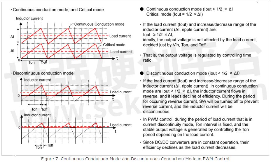
Continuous Conduction Mode
So far, based on the condition that the increasing and decreasing amount of the inductor current is same, the calculation of the output voltage is explained. This condition means that the inductor current should be continuous. Therefore, the relation between the output voltage and the time ratio which determines the output voltage described above assumes that the inductor current is continuous. This mode in which the inductor current is continuous is called the continuous conduction mode. Continuous conduction mode is true with the relation of the load current, Iout, and the increase/decrease range of the inductor current (ripple current), ΔI, is described as shown in the next formula:
Iout ≥ 1/2 × ΔI.
Here, especially, when Iout = 1/2 × ΔI is true, this is called critical mode.
Refer to Figure 7.
Discontinuous Conduction Mode
When the relation between the load current, Iout, and the increase/decrease range of the inductor current (ripple current), ΔI, is shown below, in the forced PWM mode,
Iout < 1/2 × ΔI,
the inductor current flows in reverse.
The reverse current from the inductor is a factor in efficiency loss, therefore, SW turns off to prevent the reverse current. If Iout < 1/2 × ΔI is true, then the inductor current is discontinuous in that case.
As shown in Figure 7, in PWM control of current discontinuous conduction mode, the output voltage is regulated by controlling Ton period depending on the load current. In PWM control, regardless of the load current, the frequency is constant, therefore, in the case of light load where the load current is low, the power consumed by DC/DC converters is not negligible compared to the power consumed by the load, resulting in a lower efficiency.
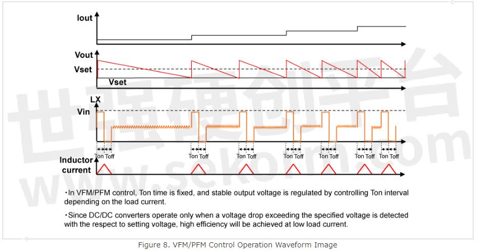
VFM/PFM Control
To improve the efficiency at light load, another control method, VFM (Variable Frequency Modulation)/PFM (Pulse Frequency Modulation) control is used. As for this control method, the output voltage is monitored, and if the output voltage becomes less than the set output threshold, the switching operation starts to provide output current to the load. On time, the pulse (Ton period), of the switching is constant, and the number of times switching occurs changes depending on the load current. If the load current is small, the interval of the pulse is long, on the contrary, if the load current is large, the interval of the pulse will be short. Since switching is only performed when a voltage drop is detected, high efficiency can be achieved at light load.
Refer to Figure 8.
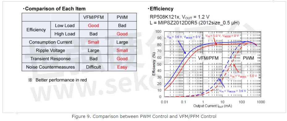
In the table on the left side of Figure 9, the comparison between PWM control and VFM/PFM control is shown. The mainstream of DC/DC converters is to use PWM control for stable operation at heavy load current and to switch to VFM/PFM control for efficiency at light load.
Comparison between PWM Control and VFM/PFM Control
Efficiency:
In PWM control, regardless of the load current, the switching frequency is constant, therefore, the efficiency at light load is worse than in VFM/PFM control. In VFM/PFM control, the switching operation starts only when the output voltage becomes less than the specified level, therefore efficiency at light load is much better than the PWM control method. Refer to the graph on the right in Figure 9; the efficiency vs. output current of PWM control and VFM/PFM control is shown in the graph.
Consumption Current:
(Although overlapping with "Efficiency") PWM control operates at a constant switching frequency regardless of the load current, therefore, the current consumption is almost constant. On the other hand, VFM/PFM control changes the switching frequency depending on the load current, therefore, the current consumption can be reduced at light load especially.
Ripple Voltage:
When compared to discontinuous conduction mode, PWM control provides current during the Ton period depending on the load current, therefore, the output ripple voltage is suppressed to a small level. VFM/PFM control aims to improve efficiency by increasing the switching interval with a constant Ton period, and the Ton period is set relatively long, therefore, the output ripple voltage is large.
Transient Response:
In the PWM control type, Ton time varies depending on the load current variation. Therefore, the transient response of PWM control is better than that of VFM/PFM control which has a fixed Ton time.
Noise:
Because DC/DC converters regulate the output voltage by switching operation, switching noise is generated. The switching noise caused by PWM control is determined by switching frequency, therefore, it is easy to design filters to take a countermeasure. However, in VFM/PFM control, the switching frequency varies depending on the load current, therefore, taking a countermeasure may be difficult.
Conclusion
I explained that by connecting the power source, inductor, and switches in different ways, and by storing energy in the inductor or release from the inductor, boosting DC/DC converters which make higher voltage than input voltage, or inverting DC/DC converters which make negative voltage can be implemented. I also explained the features of PWM control and VFM/PFM control as control methods.
In the next volume, I will explain other control methods of DC/DC converters.
Thank you for reading.
- |
- +1 赞 0
- 收藏
- 评论 0
本文由FY转载自NISSHINBO Blogs,原文标题为:What Is a DC/DC Converter? Part 3,本站所有转载文章系出于传递更多信息之目的,且明确注明来源,不希望被转载的媒体或个人可与我们联系,我们将立即进行删除处理。
相关推荐

What Is a DC/DC Converter? Part 4
Hello, everyone, in this volume, I will compare and explain the features of synchronous and nonsynchronous (diode) rectification methods of DC/DC converters.As a function of DC/DC converters, the actual historical order is as follows: nonsynchronous (diode) rectification→ synchronous rectification with reverse current protection (normal PWM)→ synchronous rectification without reverse current protection (forced PWM).

What Is a DC/DC Converter? Part 2
This time, I explained that the efficiency, which is the greatest feature of DC/DC converters, can be realized by utilizing the energy storage and release of the inductor, which is a component of DC/DC converters. We also addressed applications of linear regulators and DC/DC converters by comparing them.

What Is a DC/DC Converter? Part 5
In these five volumes on DC/DC converters, I have mainly taken non-isolated DC/DC converters as examples, and only the basics of the converters have been mentioned. As for isolated DC/DC converters, I have only explained flyback converter as an example. I would say that we are just getting to know about the fundamental concepts of DC/DC converters.

带同步整流器的RP509x系列0.5A/1A PWM/VFM降压DC/DC变换器
描述- 该资料介绍了RP509x系列低功耗PWM/VFM降压型DC/DC转换器,具有同步整流功能。该产品适用于便携式通信设备、锂离子电池供电设备等,提供固定或可调输出电压选项,并具备多种保护电路。
型号- RP509N242A,RP509N121A,RP509Z211B,RP509Z102B,RP509Z332B,RP509Z102A,RP509Z211A,RP509Z332A,RP509Z061B,RP509Z291B,RP509Z182B,RP509N091B,RP509Z061A,RP509Z182A,RP509Z291A,RP509X,RP509N241B,RP509N132B,RP509N241A,RP509N091A,RP509N,RP509N231A,RP509N122A,RP509N122B,RP509Z321B,RP509Z062B5,RP509Z212A,RP509Z321A,RP509Z212B,RP509Z062A,RP509Z171B,RP509Z171A,RP509Z062B,RP509Z292A,RP509Z292B,RP509Z,RP509N121B,RP509N242B,RP509N092A,RP509N092B,RP509NXXXB,RP509Z00XC,RP509Z00XD,RP509Z201A,RP509Z322A,RP509Z201B,RP509Z322B,RP509NXXXA,RP509Z172A,RP509Z132B5,RP509Z172B,RP509Z281A,RP509Z281B,RP509N251A,RP509N142A,RP509N142B,RP509N251B,RP509Z202A,RP509N132A,RP509Z061B5,RP509Z311A,RP509Z202B,RP509Z311B,RP509Z282A,RP509Z161A,RP509Z161B,RP509Z282B,RP509N131A,RP509N252B,RP509N252A,RP509N131B,RP509N222A,RP509Z312A,RP509N101A,RP509N101B,RP509N331B,RP509N331A,RP509N222B,RP509ZXX2B,RP509ZXX2A,RP509Z312B,RP509N131B5,RP509Z271A,RP509Z162B,RP509Z162A,RP509Z131B5,RP509Z271B,RP509N071A,RP509N192A,RP509N071B,RP509N192B,RP509N211A,RP509N102A,RP509N332A,RP509Z301A,RP509N102B,RP509N211B,RP509N332B,RP509ZXX1B,RP509ZXX1A,RP509Z301B,RP509Z272A,RP509X SERIES,RP509Z272B,RP509Z151B,RP509Z151A,RP509N072A,RP509N181A,RP509N072B,RP509N111X5,RP509N181B,RP509Z302A,RP509Z302B,RP509N111A,RP509N232B,RP509N232A,RP509N111B,RP509N002C,RP509X00XC,RP509X00XD,RP509Z261A,RP509Z152A,RP509Z261B,RP509Z152B,RP509N001C,RP509N231B,RP509N001D,RP509N081A,RP509ZXXX$-E2-F,RP509N081B,RP509N112A,RP509N221B,RP509N112B,RP509N221A,RP509Z141A,RP509Z262B,RP509Z262A,RP509Z141B,RP509N002D,RP509N082A,RP509N191A,RP509N082B,RP509N191B,RP509N202A,RP509N311B,RP509NXX1B,RP509N311A,RP509N202B,RP509Z251B,RP509Z142B,RP509Z142A,RP509Z251A,RP509N172A,RP509N281B,RP509N172B,RP509N281A,RP509NXXX$-TR-FE,RP509N312A,RP509N312B,RP509Z131B,RP509Z131A,RP509Z252A,RP509Z252B,RP509N282A,RP509N161A,RP509N161B,RP509N282B,RP509N321A,RP509N212B,RP509N212A,RP509N321B,RP509Z132A,RP509N132B5,RP509Z132B,RP509Z241A,RP509Z241B,RP509Z091A,RP509Z091B,RP509N061A,RP509N291A,RP509N182A,RP509N061B,RP509N182B,RP509N291B,RP509ZXXXA,RP509N00XC,RP509N00XD,RP509N201B,RP509N322B,RP509N201A,RP509N322A,RP509ZXXXB,RP509Z242A,RP509Z121A,RP509Z121B,RP509Z242B,RP509Z092B,RP509Z092A,RP509N062A,RP509N171A,RP509N062B,RP509N292B,RP509N292A,RP509N171B,RP509Z231A,RP509Z122B,RP509Z122A,RP509Z001D,RP509Z001C,RP509Z231B,RP509Z081B,RP509Z081A,RP509Z112B5,RP509N152A,RP509N261B,RP509N152B,RP509N261A,RP509XXXXA,RP509Z232A,RP509Z232B,RP509Z111B,RP509Z002C,RP509XXXXB,RP509Z111A,RP509Z002D,RP509Z082A,RP509Z191B,RP509Z101B5,RP509Z191A,RP509Z082B,RP509N262A,RP509N141A,RP509N141B,RP509N262B,RP509N301A,RP509N301B,RP509Z221A,RP509Z112A,RP509N111B5,RP509Z221B,RP509Z112B,RP509Z071A,RP509Z192A,RP509Z071B,RP509Z192B,RP509N271A,RP509N162A,RP509N162B,RP509N271B,RP509N302B,RP509N302A,RP509NXX2B,RP509Z101A,RP509Z331A,RP509Z222B,RP509Z331B,RP509N111A5,RP509Z222A,RP509Z101B,RP509Z181A,RP509Z072B,RP509Z072A,RP509Z181B,RP509N151A,RP509N272B,RP509N272A,RP509N151B
RP602x系列1.5 A PWM/VFM Buck-Boost同步整流DC/DC变换器
描述- RP602x系列是一款6.5V(最大额定值)的同步整流Buck-Boost DC/DC转换器,适用于工业或OA设备,即使在低输入电压(最小2.3V)下也能实现恒定电压。该设备具有高效率、小尺寸和低功耗的特点,适用于便携式设备、Li-ion电池设备等多种应用。
型号- RP602Z375C,RP602K305E,RP602K305F,RP602Z375D,RP602Z375A,RP602Z375B,RP602K360H,RP602K360F,RP602K360G,RP602K275G,RP602K360E,RP602K275H,RP602K275E,RP602K275F,RP602K415F,RP602Z350A,RP602K415E,RP602KXXXD,RP602KXXXC,RP602KXXXB,RP602Z350D,RP602Z350B,RP602Z350C,RP602K385G,RP602K385H,RP602Z415B,RP602K385E,RP602Z415C,RP602K385F,RP602Z415A,RP602ZXXX$-E2-F,RP602K305G,RP602Z415D,RP602X330X,RP602K305H,RP602Z385B,RP602Z385C,RP602Z385A,RP602Z385D,RP602K350G,RP602X290X,RP602K350H,RP602K350E,RP602K350F,RP602Z305A,RP602Z305C,RP602Z305B,RP602Z305D,RP602K415H,RP602K415G,RP602Z275A,RP602K405G,RP602K405F,RP602Z275C,RP602K405E,RP602Z275B,RP602Z360C,RP602Z275D,RP602Z360D,RP602Z360A,RP602Z360B,RP602X SERIES,RP602K375H,RP602K375F,RP602K375G,RP602K375E,RP602X320X,RP602Z395A,RP602Z395B,RP602Z400D,RP602Z395C,RP602Z395D,RP602K340H,P602KXXXA,RP602K340F,RP602K340G,RP602K340E,RP602Z315B,RP602Z315A,RP602Z400B,RP602Z315D,RP602Z315C,RP602Z400C,RP602Z400A,RP602K405H,RP602Z285B,RP602Z285A,RP602Z370B,RP602Z285D,RP602Z285C,RP602Z370C,RP602Z370A,RP602Z370D,RP602X350X,RP602K365G,RP602K365H,RP602K365E,RP602K365F,RP602Z410C,RP602Z410D,RP602K330G,RP602K330H,RP602K330E,RP602Z325A,RP602K330F,RP602Z410A,RP602Z325D,RP602Z410B,RP602Z325B,RP602Z325C,RP602Z300D,RP602Z300C,RP602Z295A,RP602Z380A,RP602Z295C,RP602Z295B,RP602Z380B,RP602Z295D,RP602Z380C,RP602Z380D,RP602K290H,RP602K290F,RP602K290G,RP602K290E,RP602K355H,RP602K355F,RP602K355G,RP602K355E,RP602Z300B,RP602Z300A,RP602X340X,RP602Z420D,RP602Z420B,RP602Z420C,RP602Z270B,RP602Z270A,RP602Z270D,RP602Z270C,RP602K320H,RP602K320F,RP602K320G,RP602X410X,RP602K320E,RP602Z335C,RP602Z420A,RP602Z335D,RP602Z335A,RP602Z335B,RP602Z310C,RP602Z310B,RP602Z310D,RP602Z390A,RP602Z390D,RP602Z390B,RP602Z390C,RP602K280G,RP602K280H,RP602K280E,RP602X370X,RP602K280F,RP602K345G,RP602K345H,RP602K345E,RP602K345F,RP602Z310A,RP602Z345D,RP602Z280A,RP602Z280C,RP602Z280B,RP602Z280D,RP602K390G,RP602K390H,RP602K390E,RP602K390F,RP602K310G,RP602K310H,RP602K310E,RP602K310F,RP602X400X,RP602Z345B,RP602Z345C,RP602Z345A,RP602Z320C,RP602Z320D,RP602Z320A,RP602Z320B,RP602K270H,RP602XXXXC,RP602X360X,RP602XXXXB,RP602K270F,RP602XXXXE,RP602K270G,RP602XXXXD,RP602XXXXG,RP602K270E,RP602XXXXF,RP602XXXXH,RP602K420H,RP602K420G,RP602K420F,RP602K335H,RP602Z330X,RP602K420E,RP602K335F,RP602K335G,RP602XXXXA,RP602K335E,RP602Z355C,RP602Z355D,RP602Z290B,RP602Z290A,RP602Z290D,RP602Z290C,RP602Z,RP602X,RP602K380H,RP602K380F,RP602K380G,RP602X280X,RP602K295G,RP602K380E,RP602K295H,RP602K295E,RP602K295F,RP602K300H,RP602K300F,RP602K300G,RP602Z355A,RP602Z355B,RP602K300E,RP602Z330B,RP602Z330C,RP602Z330A,RP602Z330D,RP602X390X,RP602K410H,RP602K410G,RP602K410F,RP602X310X,RP602K410E,RP602K325G,RP602K325H,RP602K325E,RP602K325F,RP602K,RP602Z365D,RP602K315E,RP602Z365B,RP602Z365C,RP602K370G,RP602X270X,RP602K370H,RP602K370E,RP602K285H,RP602K370F,RP602K285F,RP602K285G,RP602K285E,RP602Z365A,RP602X420X,RP602KXXX#-TR,RP602Z340A,RP602Z340B,RP602Z340C,RP602Z340D,RP602X380X,RP602K395H,RP602K395F,RP602K395G,RP602Z405C,RP602K395E,RP602Z405D,RP602Z405A,RP602K400H,RP602X300X,RP602Z405B,RP602K400G,RP602K400F,RP602K315H,RP602K400E,RP602K315F,RP602K315G
R1270S系列3 A,34 V输入PWM/VFM降压DC/DC变换器,带PLL同步
描述- R1270S系列是一款基于CMOS技术的降压DC/DC转换器,具有内部N沟道高边开关晶体管。该转换器可提供高达3A的输出电流,并具备PWM/VFM模式切换、自动软启动、过流保护、过压锁定等功能。其内部振荡器频率可调,支持PLL同步,适用于多种数字家电、办公设备、通信设备等。
型号- R1270S,R1270X001,R1270S001A,R1270S001B,R1270S001*-E2-FE,R1270S SERIES

NISSHINBO Launched 0.5A/1A 6MHz PWM/VFM Step-down DC/DC Converter RP539 Series with Synchronous Rectifier
The RP539 Series is a low-supply current CMOS-based PWM/VFM step-down DC/DC converter with a synchronous rectifier featuring 0.5A/1A output current. The RP539 Series is employing synchronous rectification for improving the efficiency of rectification by replacing diodes with built-in switching transistors.

带同步整流器的RP539Z系列0.5A/1A PWM/VFM降压DC/DC转换器
描述- 该资料介绍了已停产的RP539Z系列低功耗CMOS PWM/VFM降压型DC/DC转换器。它具有内置同步整流器和多种保护功能,适用于光通信模块、智能手机和平板电脑等便携式设备。
型号- RP539Z09XB,RP539Z20XB,RP539Z20XA,RP539Z22XB,RP539Z22XA,RP539ZXX1A,RP539Z28XB,RP539Z07XA,RP539Z28XA,RP539Z07XB,RP539ZXX1B,RP539Z09XA,RP539Z24XB,RP539Z24XA,RP539Z26XB,RP539ZXXY$-E2-F,RP539Z26XA,RP539Z32XA,RP539Z30XB,RP539ZXXXB,RP539Z11XA,RP539ZXXXA,RP539Z11XB,RP539Z32XB,RP539Z30XA,RP539ZXX2B,RP539Z17XA,RP539ZXX2A,RP539Z17XB,RP539Z19XA,RP539Z19XB,RP539Z13XA,RP539Z13XB,RP539Z15XA,RP539Z15XB,RP539Z21XA,RP539Z23XA,RP539Z21XB,RP539Z06XA,RP539Z29XA,RP539Z06XB,RP539Z27XB,RP539Z002C,RP539Z08XA,RP539Z002D,RP539Z08XB,RP539Z29XB,RP539Z00XC,RP539Z25XA,RP539Z00XD,RP539Z23XB,RP539Z27XA,RP539Z25XB,RP539Z001D,RP539Z,RP539Z31XB,RP539Z SERIES,RP539Z10XA,RP539Z31XA,RP539Z10XB,RP539Z33XB,RP539Z12XA,RP539Z33XA,RP539Z16XB,RP539Z18XA,RP539Z18XB,RP539Z001C,RP539Z12XB,RP539Z14XA,RP539Z14XB,RP539Z16XA
R1210Nxx1x系列PWM升压型DC/DC变换器
描述- 该资料介绍了R1210Nxx1x系列CMOS型PWM升压DC/DC转换器。这些转换器具有高精度、低供电电流的特点,由振荡器、PWM电路、参考电压单元、误差放大器、相补偿电路、电压检测电阻、芯片使能电路组成。此外,还包括负载瞬态控制器、低导通电阻的控制晶体管、‘LX开关’以及LX开关和输出电压保护电路。该系列IC可以仅用三个外部组件(电感、二极管和电容)构成一个低纹波、高效升压DC/DC转换器。
型号- R1210N,R1210NXX1∗-TR-FE,R1210N601C,R1210N501C,R1210N601D,R1210N501D,R1210NXX1X,R1210N301X,R1210N221D,R1210N221A,R1210NXX1A,R1210N301D,R1210N301C,R1210NXX1*-TR-FE,R1210N301A
RP519Z系列0.5A/1A PWM/VFM带同步整流器的降压DC/DC变换器
描述- 该资料介绍了已停产的RP519Z系列低功耗CMOS PWM/VFM降压型DC/DC转换器。它具有同步整流功能,可提高效率并减少元件数量。产品支持多种输入电压范围和输出电压设置选项,具备电流限制和保护电路,适用于便携式通信设备和锂离子电池供电设备。
型号- RP519Z14XB,RP519Z16XA,RP519Z16XB,RP519Z18XA,RP519Z18XB,RP519Z31XA,RP519Z10XA,RP519Z31XB,RP519ZXXXB,RP519Z10XB,RP519Z33XB,RP519ZXXXA,RP519Z12XA,RP519Z33XA,RP519Z12XB,RP519Z14XA,RP519Z26XA,RP519Z26XB,RP519Z28XA,RP519Z28XB,RP519Z09XB,RP519Z09XA,RP519Z20XA,RP519Z07XB,RP519Z20XB,RP519Z07XA,RP519Z22XA,RP519Z22XB,RP519Z24XA,RP519Z24XB,RP519Z15XA,RP519Z15XB,RP519Z17XA,RP519Z17XB,RP519Z SERIES,RP519Z19XA,RP519Z19XB,RP519Z30XA,RP519Z30XB,RP519Z32XA,RP519Z11XA,RP519Z11XB,RP519Z32XB,RP519Z13XA,RP519Z13XB,RP519Z00XD,RP519Z25XB,RP519Z00XC,RP519Z27XA,RP519Z27XB,RP519Z29XA,RP519Z29XB,RP519Z08XB,RP519Z08XA,RP519Z21XA,RP519Z06XB,RP519Z21XB,RP519Z06XA,RP519Z23XA,RP519Z23XB,RP519ZXXX$-E2-F,RP519Z25XA,RP519Z
R1286K系列2通道用于AMOLED/LCD的同步整流PWM升压/逆变DC/DC转换器
描述- 该资料介绍了R1286K系列双通道PWM升压/反激式DC/DC转换器,适用于AMOLED和LCD显示屏电源。它包含一个升压DC/DC转换器和一个小信号反激式DC/DC转换器。升压转换器可产生4.6V至5.8V的可选输出电压,而反激转换器则提供-2.0V至-6.0V的可选负电压,可通过单线接口动态调整。
型号- R1286K111M,R1286K010E,R1286K002J,R1286K103M,R1286K,R1286K107C,R1286K109F,R1286K004A,R1286K008E,R1286K1XXX,R1286K002E,R1286K103G,R1286K$XX*-TR,R1286K002A,R1286K006F,R1286K SERIES,R1286KXXXN,R1286KX05A,R1286KXXXX,R1286KXXXD,R1286KXXXE,R1286K005A,R1286K007C,R1286KXXXC,R1286K009F,R1286KX02A,R1286KXXXA,R1286K0XXX,R1286KXXXL,R1286KXXXM,R1286KXXXJ,R1286K003G,R1286KXXXK,R1286KXXXH,R1286KXXXF,R1286K001B,R1286KXXXG
R1208x系列PWM低电源电流升压DC/DC变换器
描述- R1208x系列是一款低功耗CMOS PWM控制升压DC/DC转换器,适用于LED背光驱动。该产品具有低输入电压范围、低静态电流、高效率等特点,可提供恒定电流驱动LED,并可通过PWM信号调节LED亮度。产品内置过压保护、欠压锁定、过热保护等保护电路,适用于便携式设备、平板电脑和笔记本电脑的LCD显示屏LED背光驱动。
型号- R1208KX12X,R1208X SERIES,R1208X,R1208K112B,R1208X312B,R1208X312A,R1208K312A,R1208K212B,R1208K112A,R1208K212A,R1208K312B,R1208KX12A,R1208KX12B,R1208K112∗,R1208K212∗,R1208K312X,R1208K312∗,R1208KX12∗-TR

NISSHINBO‘s 600nA Low Quiescent Current Boost DC/DC Converter for Energy Harvester
NISSHINBO‘s R1810 Series is a boost DC/DC converter for electrical power storage devices, specially dedicated to 1 cell photovoltaic energy harvester since the start-up voltage is Typ. 0.35V.This product can start up with only 9µW and is applicable for charging 1 cell photovoltaic element.
RN5RK系列VFM升压型DC/DC变换器
描述- 该资料介绍了RN5RK系列升压DC/DC转换器IC的特性、应用和电气特性。这些芯片基于CMOS技术,具有超低供电电流和高输出电压精度。它们适用于电池供电设备、相机、摄像机、录像机和手持通信设备的电源。
型号- RN5RKXX1X,RN5RKXX1A SERIES,RN5RKXX1B SERIES,RN5RK502A,RN5RK501A,RN5RK501B,RN5RK301A,RN5RKXX*$-TR-FE,RN5RK302A,RN5RK SERIES,RN5RKXX2A SERIES,RN5RK,RN5RK301B,RN5RKXX2A,RN5RKXX1A,RN5RKXX1B

电子商城

现货市场

服务
可定制电感最大电流100A,尺寸最小7 x 7 x 3.0mm到最大35 x 34 x 15.5 mm,工作频率100KHZ ~ 2MHZ,感值范围:0.15 ~ 100uh;支持大功率电感,扁平线电感,大电流电感,高频电感,汽车电感器,车规电感,一体成型电感等定制。
最小起订量: 5000 提交需求>
授权代理品牌:集成电路


授权代理品牌:分立元件


授权代理品牌:接插件及结构件


授权代理品牌:部件、组件及配件


授权代理品牌:电源及模块


授权代理品牌:电子材料


授权代理品牌:仪器仪表及测试配组件


授权代理品牌:电工工具及材料


授权代理品牌:机械电子元件


授权代理品牌:加工与定制


登录 | 立即注册
提交评论