COOLMOS Learning project




1. COOLMOS in the past
COOLMOS, also known as Super Junction MOS, has been called COOLMOS since the term Infineon is commonly used.
(Please refer to the thesis of Dr. Liu of Xi 'a Core Electronics Shanghai R&D Center and related network materials below)
In 1988, D.J.Oe of Philips America applied for the US patent no. US Pat:4754310, and proposed for the first time that, based on LDMOS structure, pn alternate structure was adopted to replace the original single light-concentration doped drift region, and the method of effectively keeping the voltage withstand of the device while lowering the on-off resistance was used to realize the super-junction device in the real sense. As shown in Figure 1, in the original traditional LDMOS drift region, the pn alternating structure replaces the single low-concentration doped drift region, and the leakage end of LDMOS is the highly doped N + region, which is directly connected to the PN alternating drift region.
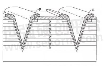
Fig.1LDMOS PN alternate structure diagram
2. Structural differences between SJ_MOS and VDMOS
To overcome the contradiction between traditional MOS conduction resistance and breakdown voltage, some people proposed a new type of ideal device structure based on VDMOS, which is called hyperjunction MOS. The structure of hyperjunction MOS is shown in Figure 2, which consists of a series of Alternate p-type and N-type semiconductor thin layers. In the cut-off state, due to the mutually compensating effect of the depletion zone electric field in the P-type and N-type layers, the doping concentration of the P-type and N-type layers can be very high without causing the drop of the device breakdown voltage. When conducting, such a high concentration of doping can make its conducting resistance significantly decreased, about two orders of magnitude. Because of this special structure, the performance of hyperjunction MOS is better than that of traditional VDMOS. It can be seen from the following table that the parameters of hyperjunction MOS of SMIC electron are better than those of planar MOS.

Fig.2 Schematic diagram of composite buffer layer structure
For conventional VDMOS device structure, the contradictory relationship between Rdson and BV should be improved by reducing EPI parameter concentration. However, the epitaxial layer is a channel for forward current flow. When EPI parameter concentration is reduced, the resistance must be increased and Rdson will be increased. Rdson directly determines the loss of the MOSFET monomer. Therefore, for ordinary VDMOS, the contradiction between the two is irreconcilable, which is the limitation of conventional VDMOS.
But with hyperjunction MOS, the contradiction is less obvious. By setting a P zone deep into the EPI, the BV is greatly improved without affecting Rdson. For conventional VDMOS, the reverse withstand voltage is mainly dependent on the PN junction between n-type EPI and body area; for a PN junction, the withstand voltage is mainly dependent on the depletion zone bearing, the size of the electric field in the depletion zone, and the area of the expansion width of the depletion zone. In conventional VDSMO, P body concentration is greater than N EPI, it should also be clear, the p-n junction depletion region mainly to the low diffusion mixed side, so this structure, the P side body area, depletion region extension is very small, basic has little contribution to pressure, pressure mainly P body - N EPI area in the side of the N type, the area of electric field intensity is a gradual change, the closer to the surface of a p-n junction, the greater the electric field intensity E. The COOLMOS structure, due to set up a relatively lower P P body concentration region area, so the P area on the side of the depletion region will greatly expand, and this area is deep in the EPI, causing the p-n junction can bear large voltage on both sides, in other words, is the peak electric field Ec by near the device surface, in areas where the device internal deeply moved.
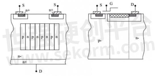
Fig.3 Tihanyi patent hyperjunction schematic diagram
- |
- +1 赞 0
- 收藏
- 评论 0
本文由三年不鸣转载自HI-SEMICON News,原文标题为:COOLMOS Learning project,本站所有转载文章系出于传递更多信息之目的,且明确注明来源,不希望被转载的媒体或个人可与我们联系,我们将立即进行删除处理。
相关研发服务和供应服务
相关推荐
SiC-MOSFET和Si-MOSFET、IGBT的区别
功率转换电路中的晶体管的作用非常重要,为进一步实现低损耗与应用尺寸小型化,一直在进行各种改良。SiC功率元器件半导体的优势如:低损耗、高速开关、高温工作等,显而易见这些优势是非常有用的。本文介绍SiC-MOSFET和Si-MOSFET、IGBT的的区别。
技术探讨 发布时间 : 2023-10-20
【技术】MOSFET规格书参数详解
极限参数HI-SEMICON极限参数也叫绝对最大额定参数,MOS管在使用过程当中,任何情况下都不能超过下图的这些极限参数,否则MOS管有可能损坏。本文对MOSFET规格书参数进行详细讲解。
技术探讨 发布时间 : 2023-11-13
【技术】VDMOS器件关键参数介绍
本文HI-SEMICON关于VDMOS器件关键参数介绍。VDMOS结构就是P型注入和N+注入后两次扩散形成P型区和N+型区,在硅表面P型区和N+型区之间形成沟道,在栅极加压后沟道开启,电流在沟道内沿表面流动,然后垂直地被漏极收集图中S为源极。
技术探讨 发布时间 : 2023-03-16
HI-SEMICON(深鸿盛)MOSFET/SiC肖特基二极管/SiC MOSFET选型指南
目录- 公司简介 MOSFET Product Introduction VDMOS 超结MOSFET 中低压MOSFET 碳化硅肖特基二极管 碳化硅MOS MOSFET/SiC肖特基二极管封装
型号- SCF60R190C,SFD3006T,SFD6003T,SGP104R5T,SFS0406T4,SFM6005DT,SFD7N70,SFW90N25,SFQ0320T4,SFD18N20,SFM4009T,SFE6001T2,SFM6004T5,SFK2N50,SFF60N06,SFN4006T5,SFM0420T4,SFP10003PT,SFF18N20,SCF65R190TF,SFD2N50,SFM4004PT,SFS6003PT,SFP33N10,SFS4010T,SGS6001T4,SGP6008T,SFS3401,SFQ0318T4,SC3D40120D,SFS3400,SFK1N65,SCD65R960C,SFS4010T2,SFF5N80,SFS0407T4,SFS3407,SFD6005T,SFD10003PT,SFD7N50,SFM6005ST,SFF18N50,SFP40P10,SGS15HR430T,SFA10015T,SFP50N06,SCF65R640C,SFD3003T,SFQ0322T4,SFF12N65,SFD6006T,SGD105R5T,SFP11P20,SFD6N70,SFS6007T,SGM10HR14T,SCF65R380C6,SFS3400.A,SFS3001T2,SCD70R600C,SFQ0420T4,SCF60R580C,SGXXXXXPT,SGM062R3T,SFS4525T,SFD3004T5,SFS3401A,SGM066R5T,SFN3009T,SGM031R7T,SFB11N90,SCD70R900C,SFU3006T,SFP9N20,SFA110P06,SFR0305T2,SFF50N06,SFD6007T,SCD80R500S,SC3D08065G,SCF65R380C,SFD4006T,SC3D08065I,SFN0315T4,SFN3003PT,SFA6005T,SFS4008T2,SFS2300,SGP157R5T,SFS2301,SFM10015T,SFH8402DW,SC3D04065E,SCU70R900C,SCF60R280C,SFS2304,SFS2303,SFF13N50,SFS2305,SC3D04065I,SFF7N50,SCF65R540T,SFD50N06,SFP20007,SFU18N20,SGP104R0T,SCD65R1K2C,SFN0330T2,SFD6008T,SGM107R7T,SC3D04065A,SFM4010T,SFF20N50,SC3D20065D,SFP40N20,SFS0307T4,SFD3012T,SFF7N65,SCD60R580C,SFU5N20,SC3D10065A,SGM105R0T,SCF65R310C,SCF60R360C6,SFS0405T4,SC3D10065G,SC3D10065I,SFP6P10,SFM4005DT,SC3K080120,SCK65R1K15C,SFW50N25,SFU4N65,SFN0413T4,SFD5N65,SFP30P10,SFM10003PT,SC3D08065A,SFP18P10,SFD4N90,SFF7N70,SCF60R125C,SFXXXXXPTX,SFD4006PT,SFD4003T,SCF70R600C,SFF6005T,SFS0306T4,SCF80R950C,SGA104R0T,SFD3010T,SFE3007T,SFD5N50,SFP3006T,SFP3018T,SFP18N20,SGP103R0T,SCW65R075CF,SCF65R170C,SFS6012T2,SGD6008T,SGM041R8T,SFD4001PT4,SFD4001PT5,SFF8N65,SFN3006PT,SC3K040120,SGM6008T,SFD4N70,SCW60R030CF,SFB50N25,SCW65R041CF,SFP6005T,SFS2013PT,SCF70R420C,SCW65R090C,SGM031R1T,SCD70R420C,SC3K075120,SFD33N10,SCW65R099TF,SFP5P03,SCF60R160C,SFR0206T2,SFD4N65,SC3D15120H,SFS2N7002,SFF33N10,SCF70R360C6,SFD2008T,SFN3003T,SFS2302B,SGM109R5T,SFM6008T,SFD3006PT,SFD6003PT,SGA104R5T,SFF20N65,SFK4N65,SFB90N25,SFD5N20,SFR0205PT2,SGM030R7T,SFF8N80,SC3D30065D,SFN3002T,SFU9N20,SFD7N65E,SFD9N65,SFD4004PT,SFF20N70,SGM042R4T,SFP6007T,SFS3401B,SFS4435,SFU6003T,SGU6008T,SFM0430T2,SFF10N70,SCF60R360C,SFD2006T,SC3D06065E,SC3D06065G,SFP75P55,SC3D10120H,SFF3N80,SC3D06065A,SCD70R600C6,SCD65R380C,SFD14N25,SC3K015120,SFSAP4580,SFS6010T2,SCD65R540T,SGP105R5T,SFF4N65,SFF10N65,SC3D30120H,SFM0320T4,SC3D30120D,SC3D16065A,SC3D16065D,SC3D16065G,SFP27P20,SC3K050120,SFU6005T,SFW10P04,SFD3N50,SFF4N70,SFM10008T,SFF9N90,SCXXXXXXXXFX,SFD2003T,SFN0318T2,SFD3009T,SFM3011T,SFD6005PT,SC3K032120,SFP110N55,SFF16N65,SC3D12065A,SFF10N80,SFF5N50,SC3D12065G,SGD10HR20T,SC3D12065I,SC3D20120H,SFP59N10,SFN6004T5,SXXXXXXX,SFD9N20,SCF65R240C,SC3D06065I,SCD65R640C,SFS2012PT,SGA105R5T,SFN0250T2,SFM3012T,SC3D20120D,SGM041R3T
HI-SEMICON MOSFET在园林工具上的应用,具有优秀Rdson和EAS性能,较低FOM值
园林工具市场正经历锂电化趋势,其中无刷电机技术受到重视,MOSFET在其中扮演关键角色。深鸿盛电子提供适合园林工具的中低压MOS产品,具有优秀的性能和多种封装选择,满足不同电池供电和电机负载需求。
应用方案 发布时间 : 2024-09-15
【经验】超级结MOSFET在电源上的应用优点及问题
COOLMOS的前世今生COOLMOS也就是super junction MOS由于大家习惯沿用了英飞凌的叫法,所以一直叫COOLMOS,也叫超结MOS。COLLMOS在电源上应用的优点有通态阻抗小,通态损耗小、同等功率规格下封装小,有利于功率密度的提高、棚电荷小,对电路的驱动能力要求降低、节电容小,开关速度加快,开关损耗小。
设计经验 发布时间 : 2022-12-15
HI-SEMICON(深鸿盛)场效应管(MOSFET)选型表
目录- 中低压功率MOSFETs 高压功率MOSFETs 超结MOSFETs
型号- SFU6007T,SFP20N65,SCF60R190C,SFD3006T,SFD6003T,SGP104R5T,SFF10N65R,SFD7N70,SFF4N60E,SFQ0320T4,SFM4009T,SFE6001T2,SFP20N60,SFK2N50,SFF60N06,SFM041R8T,SFD60N06,SFD2N50,SFP4N65,SFP33N10,SFP4N65E,SCP60R190C,SFP20N70,SFS3401,SFD4N60E,SFS3400,SFD6005T,SFD7N65E-Y,SFD7N50,SFM6005ST,SFF18N50,SCA60R280C,SFM4N65,SFD1N65,SCP70R360C6,SFD3015T,SGA855R0T,SFP50N06,SCA65R540T,SCF65R640C,SFQ0322T4,SFU4N65E,SFF12N65,SFD6006T,SFD6N70,SGM10HR14T,SFQ0420T4,SGM062R3T,SFS4525T,SFD3N50-P,SFN3009T,SCD60R360C,SFF6N70,SFU3006T,SCF65R1K15C,SFP9N20,SFF50N06,SFD6007T,SFF3N50-P,SFP10N60,SCF65R380C,SFP7N65E-Y,SCP65R380C,SCP60R280C,SFS4008T2,SFS2300,SFF7N65-Y,SCF60R280C,SFF13N50,SFF7N50,SCF65R540T,SFD50N06,SFP10N70,SCD65R1K2C,SFM4010T,SFD3N50TS,SFF6007T,SCF80R500C,SCD80R500C,SFF2N50,SFD3012T,SFA3018T,SFF7N65,SCF65R310C,SFF7N65E-Y,SCD70R360C6,SFF6006T,SCK65R1K15C,SFD4N65E,SFF15N10,SFU4N65,SFF7N70,SFD4003T,SFU9N65,SFF6005T,SFD7N65-Y,SCP60R160C,SCA60R190C,SCF80R950C,SFK3N50,SCF55R2K7C,SFF12N65-Y,SFE3007T,SFP3006T,SFD5N50,SGM6005DT,SFF9N20,SGF15N10,SFP60N06,SFS2N10,SCF70R600C6,SFD4001PT5,SFP10N65-Y,SFF3N50,SFM4N65E,SCD65R125C,SCF65R125C,SFD4N70,SFP7N65-Y,SFF5N50TS,SFP6005T,SCP65R125C,SGM031R1T,SCF70R420C,SCD70R420C,SFP12N65-Y,SCP65R540T,SCF60R160C,SFD4N65,SFS2N7002,SFF3N50TS,SFF33N10,SCF70R360C6,SFS2302B,SFS2301B,SFD15N10,SFF20N60,SFD6003PT,SGA104R5T,SFF20N65,SFS4606T,SFU4003T,SGD15N10,SFF9N50,SFD10N65-J,SFF4N65E,SFD4004PT,SFD9N65,SFF20N70,SFU10N65R,SCD55R2K7C,SFU6003T,SFF10N70,SCF60R360C,SFD2006T,SFF9N65,SFP13N50,SCD70R600C6,SFU7N70,SCD65R380C,SFD5N50TS,SFAP4580,SFF10N60,SCD65R540T,SCP60R360C,SFF4N65,SFM0320T4,SCF65R1K2C,SCP80R500C,SGP855R0T,SFU6005T,SFD10N65R,SFD3N50,SFP12N65,SFU6N70,SFU4N60E,SFF4N70,SFF10N65-Y,SFF9N90,SGU15N10,SFM3011T,SFF16N65,SFP110N55,SFU6006T,SFP18N50,SFU15N10,SFF5N50,SFF10N65-J,SFN6004T5,SFP59N10,SFD9N20,SCF65R240C,SCD65R640C,SFM3012T,SFS5N10S,SFN0250T2,SCD65R1K15C
HI-SEMICON中低压功率MOSFET选型表
HI-SEMICON提供中低压功率MOSFET以下参数选型,VDS[max] (V):-200~200V,ID[max](25℃) (A):-140~450A
|
产品型号
|
品类
|
Package
|
Channel
|
VDS[max] (V)
|
VGS(V)
|
ID[max](25℃) (A)
|
PD[25℃] (W)
|
VGS(th)[min] (V)
|
VGS(th)[max] (V)
|
RDS(on)[typ] (@4.5V) (Ω)
|
Ciss(typ)(pF)
|
QG[typ](nC)
|
|
SFS2302B
|
中低压功率MOSFETs
|
SOT-23-3L
|
N
|
20
|
±10
|
2.8
|
0.35
|
0.55
|
1.2
|
45
|
286
|
32.8
|
选型表 - HI-SEMICON 立即选型
HI-SEMICON高压功率MOSFET选型表
HI-SEMICON提供高压功率MOSFET以下参数选型,VDS[max] (V):55~1500V,ID[max](25℃) (A):1~110A
|
产品型号
|
品类
|
Package
|
Channel
|
VDS[max] (V)
|
VGS(V)
|
ID[max](25℃) (A)
|
PD[25℃] (W)
|
VGS(th)[min] (V)
|
VGS(th)[max] (V)
|
RDS(on)[typ] (@10V) (Ω)
|
Ciss(typ)(pF)
|
QG[typ](nC)
|
|
SFF7N65-Y
|
高压功率MOSFETs
|
TO-220F-3L
|
N
|
650
|
±20
|
50
|
62
|
2.0
|
4.0
|
15.4
|
1530
|
41.7
|
选型表 - HI-SEMICON 立即选型
HI-SEMICON提供用于电子烟DCDC电源的中低压MOSFET,具有较低栅极电荷及导通电阻
电子烟作为传统烟草的替代品也越来越为人们接受,雾化器内置的DCDC电源作为电子烟的核心部件通过加热烟油从而起到传统烟草的效果。中低压MOSFET作为DCDC电源的核心部件,其性能对整个电子烟的性价比有着至关重要的影响。
应用方案 发布时间 : 2023-11-09
电子商城
现货市场
服务
定制液冷板尺寸5mm*5mm~3m*1.8m,厚度2mm-100mm,单相液冷板散热能力最高300W/cm²。
最小起订量: 1片 提交需求>
可根据用户的MOSFET管进行参数检测出具报告,静态参数最大电压:7500V、检测最大电流6000A;动态参数最大电压:3300V、检测最大电流:4500A。该测试标准满足GB、IEC及行业标准等,具备可靠性评估及老化实验能力。
实验室地址: 西安 提交需求>





登录 | 立即注册
提交评论