Details of MOS tube packaging


After the MOS tube chip is made, a shell is needed to be added to the MOS tube chip, which is the MOS tube package. The package housing mainly plays the role of support, protection and cooling, and also provides electrical connection and isolation for the chip, so as to form a complete circuit between MOS tube devices and other components. Different packaging, different design, MOS tube specifications, size, various electrical parameters, etc. will be different, and they can play a different role in the circuit will be different; In addition, packaging is also an important reference for MOS tube selection in circuit design. The importance of encapsulation is self-evident.
MOS tube packaging classification
MOS tube packages can be divided into two main categories according to the way they are installed on THE PCB: Through Hole and Surface Mount.
The insertion type is the MOSFET pin that passes through the mounting hole of the PCB and is welded to the PCB. The plug-in package has a transistor profile package (TO).
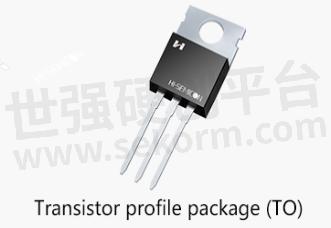
Fig.1 Plug in package
Surface mount is MOSFET pin and heat dissipation flange welding on the PCB surface of the solder pad. Typical surface-mounted packages include: D-PAK, SOT, SOP, etc. With the development of technology, fewer and fewer PCB boards, such as motherboards and video CARDS, adopt the straight-insert packaging mode, and more and more surface mount packaging mode is adopted.

Fig.2 Surface mount packaging
1. Dual inline package (DIP)
The DIP package has two rows of pins, which need to be inserted into the chip socket with the DIP structure, and is derived from SDIP(Shrink), that is, the double-wire package is six times more dense than the DIP pin density.
DIP packaging structure forms include: multilayer ceramic double-row DIP, single-layer ceramic double-row DIP, lead frame DIP(including glass ceramic sealing type, plastic sealing structure type, ceramic low-melt glass packaging type). The DIP package features easy perforation welding of the PCB and good compatibility with the motherboard. But because its package area and thickness are relatively large, and pin is easy to be damaged in the process of plugging, the reliability is poor; At the same time, due to the influence of the process, there are generally no more than 100 pins, so in the highly integrated process of the electronics industry, DIP packaging gradually withdrew from the historical stage.
2. Transistor shape Packaging (TO)
It belongs TO the early packaging specifications, such as TO-3P, TO-247, TO-220, TO-220F, TO-251, to-263, etc., are all plug-in packaging designs.
TO-3P /247: It is the commonly used packaging form of medium and high voltage, large current MOS tube. The product has the characteristics of high voltage resistance, strong resistance TO wear, etc.
TO-220 /220F: TO-220F is fully plastic package. There is no need TO add insulation pad when it is installed on the radiator. The TO-220 has a metal strip attached TO the middle foot and an insulating pad for the radiator. The two encapsulated MOS tubes are similar in appearance and can be used interchangeably.
TO-251: The packaged product is designed TO reduce cost and reduce volume, and is mainly used in medium voltage environment with large current below 60A and high voltage below 7N.
In recent years, due TO the high welding cost of plug-in packaging process and the lower heat dissipation performance than SMT products, the market demand for SURface-mount packaging has been increasing, which also leads TO the development of TO packaging TO SURface-mount packaging. To-252 (also known as D-PAK) and to-263 (D2PAK) are surface mount packages.
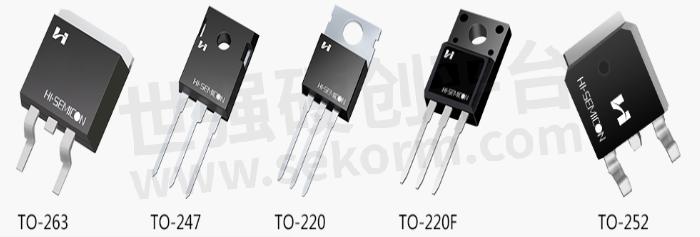
Fig.3 TO encapsulate the appearance of a product
TO-252 is a kind of plastic chip packaging, often used in the power transistor, voltage regulator chip packaging, is one of the mainstream packaging.
The MOSFET with the encapsulated mode has three electrodes, gate (G), drain (D) and source (S).
The pin of drain pole (D) is not cut, but the heat dissipation plate on the back is used as drain pole (D), which is directly welded to the PCB. On the one hand, it is used to output large current, and on the other hand, it can dissipate heat through THE PCB. Therefore, there are three d-PAK pads in PCB, and the drain pole (D) pad is larger. Its packaging specifications are as follows:
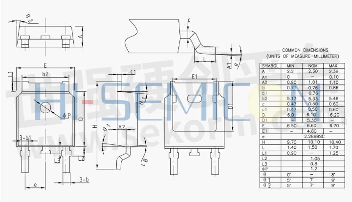
Fig.4 TO-252 Package size specification drawing
TO-263, a variant of TO-220, is designed TO improve production efficiency and heat dissipation, and supports extremely high current and voltage. It is more common in MEDIUM-voltage and high-current MOS tubes of less than 150A and more than 30V.In addition TO D2PAK(TO-263AB), also includes TO263-2, TO-263-3, TO-263-5, TO-263-7 and other styles, and TO-263 for the dependency relationship, mainly lead TO the number of feet and distance is different.
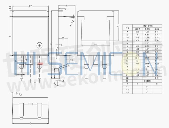
Fig.5 TO-263 Package size specification drawing
Small shape transistor Package (SOT)
The SOT(Small-Out-of-line transistorized) is a Small power transistorized sugar-patch type consisting of SOT-23-6L and SOT-23-3L, whose volume is smaller than that of TO.
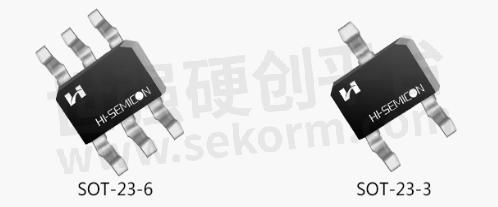
Fig.6SOT encapsulates the type diagram
SOT-23 is a common triode packaging forms, there are three wing shape pins, the collector and emitter and the base, respectively, in components on both sides of long sides respectively, among them, the emitter and the base on the same side, common in small power transistors, field effect tube and the compound transistor with resistance network, good strength, but poor weldability, shape of (a) as shown in the diagram below.
Small Shape Packaging (SOP)
SOP(Small-out-of-line Package) is one of the surface-mounted packages, also known as SOL or DFP. The pins are drawn from both sides of the Package in the shape of a seagull wing (L-shaped). There are plastic and ceramic materials.
SOP packaging standards include SOP-8, SOP-16, SOP-20, SOP-28, etc. The number after SOP represents the number of pins. MOSFET's SOP packaging mostly USES the SOP-8 specification, and the industry often omits the "P" and abbreviates it as SO(small-out-of-line).
SOP-8 package dimensions
SOP-8 is the first developed by PHILIP company. It adopts plastic package, no heat dissipation baseplate, poor heat dissipation, generally used for low power MOSFET.
After that, TSOP(thin and small shape packaging), VSOP(very small shape packaging), SSOP(reduced type SOP), TSSOP(thin and reduced type SOP) and other standard specifications are gradually derived. TSOP and TSSOP are commonly used in MOSFET encapsulation.
- |
- +1 赞 0
- 收藏
- 评论 0
本文由三年不鸣转载自HI-SEMICON News,原文标题为:Details of MOS tube packaging,本站所有转载文章系出于传递更多信息之目的,且明确注明来源,不希望被转载的媒体或个人可与我们联系,我们将立即进行删除处理。
相关研发服务和供应服务
相关推荐
SiC-MOSFET和Si-MOSFET、IGBT的区别
功率转换电路中的晶体管的作用非常重要,为进一步实现低损耗与应用尺寸小型化,一直在进行各种改良。SiC功率元器件半导体的优势如:低损耗、高速开关、高温工作等,显而易见这些优势是非常有用的。本文介绍SiC-MOSFET和Si-MOSFET、IGBT的的区别。
MOSFET芯片薄化工艺(BGBM)
客户晶圆完成入站检验后,依照客户晶圆特性,与前段晶圆代工厂所生产的护层确认所需使用之胶带后,进行胶带贴附 (Taping);接着,进行一般研磨 (Non-Taiko Grinding / Conventional Grinding),并在完成一般研磨后,进行晶背湿蚀刻 (Backside Wet Etching);最后,进行厚度量测 (Measurement) 后,出站检验。
【技术】MOSFET规格书参数详解
极限参数HI-SEMICON极限参数也叫绝对最大额定参数,MOS管在使用过程当中,任何情况下都不能超过下图的这些极限参数,否则MOS管有可能损坏。本文对MOSFET规格书参数进行详细讲解。
HI-SEMICON(深鸿盛)MOSFET/SiC肖特基二极管/SiC MOSFET选型指南
目录- 公司简介 MOSFET Product Introduction VDMOS 超结MOSFET 中低压MOSFET 碳化硅肖特基二极管 碳化硅MOS MOSFET/SiC肖特基二极管封装
型号- SCF60R190C,SFD3006T,SFD6003T,SGP104R5T,SFS0406T4,SFM6005DT,SFD7N70,SFW90N25,SFQ0320T4,SFD18N20,SFM4009T,SFE6001T2,SFM6004T5,SFK2N50,SFF60N06,SFN4006T5,SFM0420T4,SFP10003PT,SFF18N20,SCF65R190TF,SFD2N50,SFM4004PT,SFS6003PT,SFP33N10,SFS4010T,SGS6001T4,SGP6008T,SFS3401,SFQ0318T4,SC3D40120D,SFS3400,SFK1N65,SCD65R960C,SFS4010T2,SFF5N80,SFS0407T4,SFS3407,SFD6005T,SFD10003PT,SFD7N50,SFM6005ST,SFF18N50,SFP40P10,SGS15HR430T,SFA10015T,SFP50N06,SCF65R640C,SFD3003T,SFQ0322T4,SFF12N65,SFD6006T,SGD105R5T,SFP11P20,SFD6N70,SFS6007T,SGM10HR14T,SCF65R380C6,SFS3400.A,SFS3001T2,SCD70R600C,SFQ0420T4,SCF60R580C,SGXXXXXPT,SGM062R3T,SFS4525T,SFD3004T5,SFS3401A,SGM066R5T,SFN3009T,SGM031R7T,SFB11N90,SCD70R900C,SFU3006T,SFP9N20,SFA110P06,SFR0305T2,SFF50N06,SFD6007T,SCD80R500S,SC3D08065G,SCF65R380C,SFD4006T,SC3D08065I,SFN0315T4,SFN3003PT,SFA6005T,SFS4008T2,SFS2300,SGP157R5T,SFS2301,SFM10015T,SFH8402DW,SC3D04065E,SCU70R900C,SCF60R280C,SFS2304,SFS2303,SFF13N50,SFS2305,SC3D04065I,SFF7N50,SCF65R540T,SFD50N06,SFP20007,SFU18N20,SGP104R0T,SCD65R1K2C,SFN0330T2,SFD6008T,SGM107R7T,SC3D04065A,SFM4010T,SFF20N50,SC3D20065D,SFP40N20,SFS0307T4,SFD3012T,SFF7N65,SCD60R580C,SFU5N20,SC3D10065A,SGM105R0T,SCF65R310C,SCF60R360C6,SFS0405T4,SC3D10065G,SC3D10065I,SFP6P10,SFM4005DT,SC3K080120,SCK65R1K15C,SFW50N25,SFU4N65,SFN0413T4,SFD5N65,SFP30P10,SFM10003PT,SC3D08065A,SFP18P10,SFD4N90,SFF7N70,SCF60R125C,SFXXXXXPTX,SFD4006PT,SFD4003T,SCF70R600C,SFF6005T,SFS0306T4,SCF80R950C,SGA104R0T,SFD3010T,SFE3007T,SFD5N50,SFP3006T,SFP3018T,SFP18N20,SGP103R0T,SCW65R075CF,SCF65R170C,SFS6012T2,SGD6008T,SGM041R8T,SFD4001PT4,SFD4001PT5,SFF8N65,SFN3006PT,SC3K040120,SGM6008T,SFD4N70,SCW60R030CF,SFB50N25,SCW65R041CF,SFP6005T,SFS2013PT,SCF70R420C,SCW65R090C,SGM031R1T,SCD70R420C,SC3K075120,SFD33N10,SCW65R099TF,SFP5P03,SCF60R160C,SFR0206T2,SFD4N65,SC3D15120H,SFS2N7002,SFF33N10,SCF70R360C6,SFD2008T,SFN3003T,SFS2302B,SGM109R5T,SFM6008T,SFD3006PT,SFD6003PT,SGA104R5T,SFF20N65,SFK4N65,SFB90N25,SFD5N20,SFR0205PT2,SGM030R7T,SFF8N80,SC3D30065D,SFN3002T,SFU9N20,SFD7N65E,SFD9N65,SFD4004PT,SFF20N70,SGM042R4T,SFP6007T,SFS3401B,SFS4435,SFU6003T,SGU6008T,SFM0430T2,SFF10N70,SCF60R360C,SFD2006T,SC3D06065E,SC3D06065G,SFP75P55,SC3D10120H,SFF3N80,SC3D06065A,SCD70R600C6,SCD65R380C,SFD14N25,SC3K015120,SFSAP4580,SFS6010T2,SCD65R540T,SGP105R5T,SFF4N65,SFF10N65,SC3D30120H,SFM0320T4,SC3D30120D,SC3D16065A,SC3D16065D,SC3D16065G,SFP27P20,SC3K050120,SFU6005T,SFW10P04,SFD3N50,SFF4N70,SFM10008T,SFF9N90,SCXXXXXXXXFX,SFD2003T,SFN0318T2,SFD3009T,SFM3011T,SFD6005PT,SC3K032120,SFP110N55,SFF16N65,SC3D12065A,SFF10N80,SFF5N50,SC3D12065G,SGD10HR20T,SC3D12065I,SC3D20120H,SFP59N10,SFN6004T5,SXXXXXXX,SFD9N20,SCF65R240C,SC3D06065I,SCD65R640C,SFS2012PT,SGA105R5T,SFN0250T2,SFM3012T,SC3D20120D,SGM041R3T
HI-SEMICON MOSFET在园林工具上的应用,具有优秀Rdson和EAS性能,较低FOM值
园林工具市场正经历锂电化趋势,其中无刷电机技术受到重视,MOSFET在其中扮演关键角色。深鸿盛电子提供适合园林工具的中低压MOS产品,具有优秀的性能和多种封装选择,满足不同电池供电和电机负载需求。
【经验】超级结MOSFET在电源上的应用优点及问题
COOLMOS的前世今生COOLMOS也就是super junction MOS由于大家习惯沿用了英飞凌的叫法,所以一直叫COOLMOS,也叫超结MOS。COLLMOS在电源上应用的优点有通态阻抗小,通态损耗小、同等功率规格下封装小,有利于功率密度的提高、棚电荷小,对电路的驱动能力要求降低、节电容小,开关速度加快,开关损耗小。
HI-SEMICON(深鸿盛)场效应管(MOSFET)选型表
目录- 中低压功率MOSFETs 高压功率MOSFETs 超结MOSFETs
型号- SFU6007T,SFP20N65,SCF60R190C,SFD3006T,SFD6003T,SGP104R5T,SFF10N65R,SFD7N70,SFF4N60E,SFQ0320T4,SFM4009T,SFE6001T2,SFP20N60,SFK2N50,SFF60N06,SFM041R8T,SFD60N06,SFD2N50,SFP4N65,SFP33N10,SFP4N65E,SCP60R190C,SFP20N70,SFS3401,SFD4N60E,SFS3400,SFD6005T,SFD7N65E-Y,SFD7N50,SFM6005ST,SFF18N50,SCA60R280C,SFM4N65,SFD1N65,SCP70R360C6,SFD3015T,SGA855R0T,SFP50N06,SCA65R540T,SCF65R640C,SFQ0322T4,SFU4N65E,SFF12N65,SFD6006T,SFD6N70,SGM10HR14T,SFQ0420T4,SGM062R3T,SFS4525T,SFD3N50-P,SFN3009T,SCD60R360C,SFF6N70,SFU3006T,SCF65R1K15C,SFP9N20,SFF50N06,SFD6007T,SFF3N50-P,SFP10N60,SCF65R380C,SFP7N65E-Y,SCP65R380C,SCP60R280C,SFS4008T2,SFS2300,SFF7N65-Y,SCF60R280C,SFF13N50,SFF7N50,SCF65R540T,SFD50N06,SFP10N70,SCD65R1K2C,SFM4010T,SFD3N50TS,SFF6007T,SCF80R500C,SCD80R500C,SFF2N50,SFD3012T,SFA3018T,SFF7N65,SCF65R310C,SFF7N65E-Y,SCD70R360C6,SFF6006T,SCK65R1K15C,SFD4N65E,SFF15N10,SFU4N65,SFF7N70,SFD4003T,SFU9N65,SFF6005T,SFD7N65-Y,SCP60R160C,SCA60R190C,SCF80R950C,SFK3N50,SCF55R2K7C,SFF12N65-Y,SFE3007T,SFP3006T,SFD5N50,SGM6005DT,SFF9N20,SGF15N10,SFP60N06,SFS2N10,SCF70R600C6,SFD4001PT5,SFP10N65-Y,SFF3N50,SFM4N65E,SCD65R125C,SCF65R125C,SFD4N70,SFP7N65-Y,SFF5N50TS,SFP6005T,SCP65R125C,SGM031R1T,SCF70R420C,SCD70R420C,SFP12N65-Y,SCP65R540T,SCF60R160C,SFD4N65,SFS2N7002,SFF3N50TS,SFF33N10,SCF70R360C6,SFS2302B,SFS2301B,SFD15N10,SFF20N60,SFD6003PT,SGA104R5T,SFF20N65,SFS4606T,SFU4003T,SGD15N10,SFF9N50,SFD10N65-J,SFF4N65E,SFD4004PT,SFD9N65,SFF20N70,SFU10N65R,SCD55R2K7C,SFU6003T,SFF10N70,SCF60R360C,SFD2006T,SFF9N65,SFP13N50,SCD70R600C6,SFU7N70,SCD65R380C,SFD5N50TS,SFAP4580,SFF10N60,SCD65R540T,SCP60R360C,SFF4N65,SFM0320T4,SCF65R1K2C,SCP80R500C,SGP855R0T,SFU6005T,SFD10N65R,SFD3N50,SFP12N65,SFU6N70,SFU4N60E,SFF4N70,SFF10N65-Y,SFF9N90,SGU15N10,SFM3011T,SFF16N65,SFP110N55,SFU6006T,SFP18N50,SFU15N10,SFF5N50,SFF10N65-J,SFN6004T5,SFP59N10,SFD9N20,SCF65R240C,SCD65R640C,SFM3012T,SFS5N10S,SFN0250T2,SCD65R1K15C
MOS Switch Tube Selection and Principle Application
When the input voltage UI changes from high to low and the MOS tube changes from the on-off state to the cut-off state, the power UDD charges the stray capacitance CL via RD, charging time constant 1=RDCL, so the output voltage UO must pass a certain delay to change from the low level to the high level.
MOSFET晶圆后端工艺 (BGBM)
晶圆完成入站检验后 (IQC),按照客户指示之种类及厚度进行靶材准备后,进入蒸镀机沉积金属 (Evaporator)。完成金属蒸镀沉积 (Metal Evaporation) 后,以Alpha Step进行随货样本片量测,再依客户需求进行产品上非破坏性XRF量测,将各层金属量测 (Measurement) 完成后,出站检验 (OQC),至此BGBM制程完成。
Miller Effect on MOS Tube Switches
The gate drive process of MOSFET can be simply understood as the charging and discharging process of the input capacitance (mainly CGS of the gate source capacitance) of the MOSFET. When THE CGS reaches the threshold voltage, MOSFET will enter the opening state.
HI-SEMICON提供用于电子烟DCDC电源的中低压MOSFET,具有较低栅极电荷及导通电阻
电子烟作为传统烟草的替代品也越来越为人们接受,雾化器内置的DCDC电源作为电子烟的核心部件通过加热烟油从而起到传统烟草的效果。中低压MOSFET作为DCDC电源的核心部件,其性能对整个电子烟的性价比有着至关重要的影响。
电子商城
现货市场
服务
可根据用户的MOSFET管进行参数检测出具报告,静态参数最大电压:7500V、检测最大电流6000A;动态参数最大电压:3300V、检测最大电流:4500A。该测试标准满足GB、IEC及行业标准等,具备可靠性评估及老化实验能力。
实验室地址: 西安 提交需求>
定制液冷板尺寸5mm*5mm~3m*1.8m,厚度2mm-100mm,单相液冷板散热能力最高300W/cm²。
最小起订量: 1片 提交需求>


登录 | 立即注册
提交评论