Miller Effect on MOS Tube Switches


The basic principle of formation of Miller platform
The gate drive process of MOSFET can be simply understood as the charging and discharging process of the input capacitance (mainly CGS of the gate source capacitance) of the MOSFET. When THE CGS reaches the threshold voltage, MOSFET will enter the opening state. When MOSFET is opened, VDS starts to decline and ID starts to rise. At this time, MOSFET enters the saturated region. However, due to Miller effect, VGS will not rise for a period of time. At this time, ID has reached the maximum, while VDS continues to decline until Miller capacitor is fully charged and VGS rises to the value of the driving voltage. At this time, MOSFET enters the resistance area, VDS completely drops and the opening ends.
Because miller capacitors prevent VGS from rising, they prevent Vds from falling, thus increasing the time to wear out. (When VGS goes up, the conduction resistance goes down, thus VDS goes down)
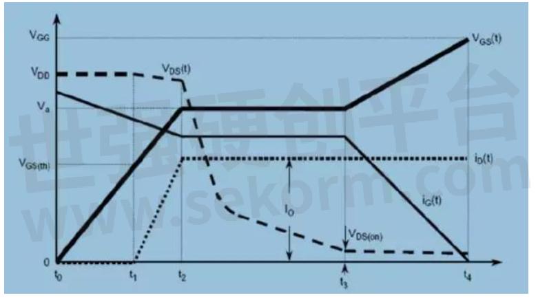
Fig.1
Miller effect is notorious in MOS drive. It is caused by the miller capacitance of the MOS tube. During the opening process of the MOS tube, the GS voltage rises to a certain voltage value and then becomes stable for some time, after which the GS voltage starts to rise again until complete conduction. Why is there a stable value here? Before the MOS is switched on, the D-pole voltage is greater than the G-pole voltage, and the electric quantity stored by the MOS parasitic capacitor CGD needs to be neutralized by the G pole injected during its conduction because the G-pole voltage is greater than the D-pole voltage after the MOS is fully switched on. The Miller effect will greatly increase the opening loss of MOS. (The MOS tube cannot be switched on very quickly)
So there comes the so-called totem drive!! When MOS is selected, the smaller the CGD is, the smaller the switching loss will be. The Miller effect is unlikely to disappear entirely.
Miller platform in MOSFET is a typical symbol of MOSFET being in the "big zone".
Using an oscilloscope to measure the GS voltage, you can see that there is a platform or pit during the voltage rise, this is the Miller platform.
The detailed process of formation of the Miller platform
The Miller effect refers to the miller platform produced in the opening process of the MOS tube switches. The principle is as follows.
In theory, the Miller effect can be eliminated by adding enough capacitance between the G and S stages of the drive circuit. But the switching time will drag on for a long time. The general recommendation plus a capacitance value of 0.1CIESS is beneficial.
The gentle part in the thick black line below is the Miller platform.
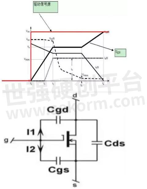
Fig.2
This diagram shows the delay-charge coefficient at the first turning point: VDS starts conduction. The variation of VDS forms a differential through CGD and the internal resistance of the driver source. Since VDS is approximately linearly decreasing, linear differentiation is a constant, resulting in a platform at VGS.
Miller platform is caused by the capacitance at both ends of MOS GD, namely CRSS in the MOS datasheet.
This process is to charge THE CGD, so the VGS changes very little. When the CGD is charged to the VGS level, the VGS will continue to rise.
When MOS was just opened, CGD discharged rapidly through MOS, and then the drive voltage was reversed charged, which Shared the drive current, making the voltage rise on CGS slow and the platform appeared.
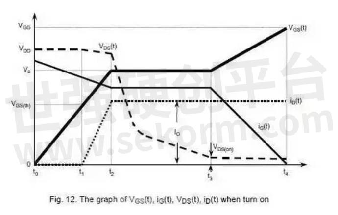
Fig.3
T0 ~ T1: VGS from 0 to VTH Mosfet not through Current by parasitic diode DF
T1 ~ T2: VGS from VTH to Va ID
T2 ~ T3: VDS decreases, The higher the current continues to pass through CGD VDD, the longer the time required.
IG is the driving current
It starts to get healthier faster When VDG approaches zero, CGD increases Until VDG becomes negative, CGD increases to the maximum IG decreases slowly
T3 ~ T4: complete conduction of Mosfet, operating in resistance zone VGS continues to rise to VGG

Fig.4
In the later stage of the platform, VGS continued to grow, and IDS changed little because MOS was saturated. However, from the picture of the building owner, this platform still had a length
During this platform, it can be considered that MOS is in the amplification period
Before the previous inflection point: MOS cutoff period, at which time CGS is charging and VGS is pressing into VTH
The previous inflection point: MOS officially entered the amplification period
At the latter inflection point, MOS officially exits the amplification period and begins to enter the saturation period
When a voltage V with a slope of it is applied to capacitance C (such as the output voltage of the driver), the current in the capacitor will be increased:
I = C x dV/dt (1)
Therefore, when voltage is applied to MOSFET, input current IGATE = I1 + I2 will be generated, as shown in the figure below:
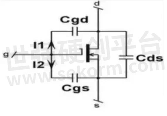
Fig.5
Using Equation (1) on the right voltage node, the following equation can be obtained:
I1 = CGD x d (VGS - VDS)/dt = CGD x (dVgs/dt - dVds/dt) (2)
I2 = CGS x d (VGS/dt) (3)
If the grid-source voltage VGS is applied to the MOSFET, the leak-source voltage VDS will drop (even in a non-linear fashion). Therefore, the negative gain of connecting the two voltages can be defined as:
Av= -VDS /VGS (4).
Substituting Equation (4) into Equation (2), we can get:
I1=CGD× (1+Av) dVgs/dt (5)
In the conversion (conduction or turn-off) process, the total equivalent capacitance Ceq of the grid-source electrode is:
IGATE = I1 + I2 = (CGD x (1 + Av) + CGS) * dVgs yet dVgs/dt = Ceq/dt (6)
The term (1+Av) is called the Miller effect, which describes the capacitive feedback between output and input in an electronic device. The Miller effect occurs when the grid-drain voltage is close to zero.
CDS diverts the most severe stage in a large area. Why? Because VD changes the most dramatically at this stage. It is precisely at this stage that the platform is formed. You can assume that the gate current IGATE is completely absorbed by the CDS and no current flows to the CGS.
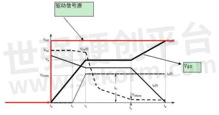
Fig.6
Note the representation in the datasheet:
CISS=CGS+CGD
COSS=CDS+CGD
CRSS=CGD
- |
- +1 赞 0
- 收藏
- 评论 0
本文由三年不鸣转载自HI-SEMICON News,原文标题为:Miller effect on MOS tube switches,本站所有转载文章系出于传递更多信息之目的,且明确注明来源,不希望被转载的媒体或个人可与我们联系,我们将立即进行删除处理。
相关研发服务和供应服务
相关推荐
【技术】MOSFET规格书参数详解
极限参数HI-SEMICON极限参数也叫绝对最大额定参数,MOS管在使用过程当中,任何情况下都不能超过下图的这些极限参数,否则MOS管有可能损坏。本文对MOSFET规格书参数进行详细讲解。
【技术】MOS管栅极、源极、漏极的定义及判定测试方法
本文深鸿盛电子带大家了解MOS管三个极定义及判断测试方法。MOS驱动器主要起波形整形和加强驱动的作用:假如MOS管的G信号波形不够陡峭,在点评切换阶段会造成大量电能损耗其副作用是降低电路转换效率,MOS管发烧严峻。
【技术】关于MOS管损坏的五种模式介绍
功率MOS管的五种损坏包括:雪崩破坏、器件发热损坏、内置二极管破坏、由寄生振荡导致的破坏、栅极电涌/静电破坏,本文详解MOS管损坏之谜。 第一种:雪崩破坏。第二种:器件发热损坏。第三种:内置二极管破坏。
HI-SEMICON(深鸿盛)MOSFET/SiC肖特基二极管/SiC MOSFET选型指南
目录- 公司简介 MOSFET Product Introduction VDMOS 超结MOSFET 中低压MOSFET 碳化硅肖特基二极管 碳化硅MOS MOSFET/SiC肖特基二极管封装
型号- SCF60R190C,SFD3006T,SFD6003T,SGP104R5T,SFS0406T4,SFM6005DT,SFD7N70,SFW90N25,SFQ0320T4,SFD18N20,SFM4009T,SFE6001T2,SFM6004T5,SFK2N50,SFF60N06,SFN4006T5,SFM0420T4,SFP10003PT,SFF18N20,SCF65R190TF,SFD2N50,SFM4004PT,SFS6003PT,SFP33N10,SFS4010T,SGS6001T4,SGP6008T,SFS3401,SFQ0318T4,SC3D40120D,SFS3400,SFK1N65,SCD65R960C,SFS4010T2,SFF5N80,SFS0407T4,SFS3407,SFD6005T,SFD10003PT,SFD7N50,SFM6005ST,SFF18N50,SFP40P10,SGS15HR430T,SFA10015T,SFP50N06,SCF65R640C,SFD3003T,SFQ0322T4,SFF12N65,SFD6006T,SGD105R5T,SFP11P20,SFD6N70,SFS6007T,SGM10HR14T,SCF65R380C6,SFS3400.A,SFS3001T2,SCD70R600C,SFQ0420T4,SCF60R580C,SGXXXXXPT,SGM062R3T,SFS4525T,SFD3004T5,SFS3401A,SGM066R5T,SFN3009T,SGM031R7T,SFB11N90,SCD70R900C,SFU3006T,SFP9N20,SFA110P06,SFR0305T2,SFF50N06,SFD6007T,SCD80R500S,SC3D08065G,SCF65R380C,SFD4006T,SC3D08065I,SFN0315T4,SFN3003PT,SFA6005T,SFS4008T2,SFS2300,SGP157R5T,SFS2301,SFM10015T,SFH8402DW,SC3D04065E,SCU70R900C,SCF60R280C,SFS2304,SFS2303,SFF13N50,SFS2305,SC3D04065I,SFF7N50,SCF65R540T,SFD50N06,SFP20007,SFU18N20,SGP104R0T,SCD65R1K2C,SFN0330T2,SFD6008T,SGM107R7T,SC3D04065A,SFM4010T,SFF20N50,SC3D20065D,SFP40N20,SFS0307T4,SFD3012T,SFF7N65,SCD60R580C,SFU5N20,SC3D10065A,SGM105R0T,SCF65R310C,SCF60R360C6,SFS0405T4,SC3D10065G,SC3D10065I,SFP6P10,SFM4005DT,SC3K080120,SCK65R1K15C,SFW50N25,SFU4N65,SFN0413T4,SFD5N65,SFP30P10,SFM10003PT,SC3D08065A,SFP18P10,SFD4N90,SFF7N70,SCF60R125C,SFXXXXXPTX,SFD4006PT,SFD4003T,SCF70R600C,SFF6005T,SFS0306T4,SCF80R950C,SGA104R0T,SFD3010T,SFE3007T,SFD5N50,SFP3006T,SFP3018T,SFP18N20,SGP103R0T,SCW65R075CF,SCF65R170C,SFS6012T2,SGD6008T,SGM041R8T,SFD4001PT4,SFD4001PT5,SFF8N65,SFN3006PT,SC3K040120,SGM6008T,SFD4N70,SCW60R030CF,SFB50N25,SCW65R041CF,SFP6005T,SFS2013PT,SCF70R420C,SCW65R090C,SGM031R1T,SCD70R420C,SC3K075120,SFD33N10,SCW65R099TF,SFP5P03,SCF60R160C,SFR0206T2,SFD4N65,SC3D15120H,SFS2N7002,SFF33N10,SCF70R360C6,SFD2008T,SFN3003T,SFS2302B,SGM109R5T,SFM6008T,SFD3006PT,SFD6003PT,SGA104R5T,SFF20N65,SFK4N65,SFB90N25,SFD5N20,SFR0205PT2,SGM030R7T,SFF8N80,SC3D30065D,SFN3002T,SFU9N20,SFD7N65E,SFD9N65,SFD4004PT,SFF20N70,SGM042R4T,SFP6007T,SFS3401B,SFS4435,SFU6003T,SGU6008T,SFM0430T2,SFF10N70,SCF60R360C,SFD2006T,SC3D06065E,SC3D06065G,SFP75P55,SC3D10120H,SFF3N80,SC3D06065A,SCD70R600C6,SCD65R380C,SFD14N25,SC3K015120,SFSAP4580,SFS6010T2,SCD65R540T,SGP105R5T,SFF4N65,SFF10N65,SC3D30120H,SFM0320T4,SC3D30120D,SC3D16065A,SC3D16065D,SC3D16065G,SFP27P20,SC3K050120,SFU6005T,SFW10P04,SFD3N50,SFF4N70,SFM10008T,SFF9N90,SCXXXXXXXXFX,SFD2003T,SFN0318T2,SFD3009T,SFM3011T,SFD6005PT,SC3K032120,SFP110N55,SFF16N65,SC3D12065A,SFF10N80,SFF5N50,SC3D12065G,SGD10HR20T,SC3D12065I,SC3D20120H,SFP59N10,SFN6004T5,SXXXXXXX,SFD9N20,SCF65R240C,SC3D06065I,SCD65R640C,SFS2012PT,SGA105R5T,SFN0250T2,SFM3012T,SC3D20120D,SGM041R3T
MOS管输出特性曲线,你看明白了吗?
我们知道,三极管是利用IB的电流去控制电流IC的,所以说三极管是电流控制电流的器件。而MOS管是利用VGS的电压去控制电流Id的,所以说MOS管是电压控制电流的器件。对于N沟道增强型的MOS管,当VGS>VGS(th)时,MOS就会开始导通,如果在D极和S极之间加上一定的电压,就会有电流Id产生。
HI-SEMICON MOSFET在无人机上的应用
无人机应用场景日益完善。无人机产品具有使用成本低、地勤保障要求低、 机动性强、安全性高、提供信息更加及时等优势,相比于传统作业方式,工业无人机更能胜任复杂环境下的作业任务。本文介绍了HI-SEMICON MOSFET在无人机上的应用。
【经验】超级结MOSFET在电源上的应用优点及问题
COOLMOS的前世今生COOLMOS也就是super junction MOS由于大家习惯沿用了英飞凌的叫法,所以一直叫COOLMOS,也叫超结MOS。COLLMOS在电源上应用的优点有通态阻抗小,通态损耗小、同等功率规格下封装小,有利于功率密度的提高、棚电荷小,对电路的驱动能力要求降低、节电容小,开关速度加快,开关损耗小。
HI-SEMICON MOSFET在园林工具上的应用,具有优秀Rdson和EAS性能,较低FOM值
园林工具市场正经历锂电化趋势,其中无刷电机技术受到重视,MOSFET在其中扮演关键角色。深鸿盛电子提供适合园林工具的中低压MOS产品,具有优秀的性能和多种封装选择,满足不同电池供电和电机负载需求。
【经验】各种开关电源MOS管驱动电路设计详解
在使用mos管驱动电路设计开关电源或者马达驱动电路的时候,大部分人都会考虑mos的导通电阻,最大电压等,最大电流等,也有很多人仅仅考虑这些因素。这样的电路也许是可以工作的,但并不是优秀的,作为正式的产品设计也是不允许的。本文介绍MOS管种类和结构,以及几个模块电源中常用的MOS管驱动电路。
HI-SEMICON(深鸿盛)场效应管(MOSFET)选型表
目录- 中低压功率MOSFETs 高压功率MOSFETs 超结MOSFETs
型号- SFU6007T,SFP20N65,SCF60R190C,SFD3006T,SFD6003T,SGP104R5T,SFF10N65R,SFD7N70,SFF4N60E,SFQ0320T4,SFM4009T,SFE6001T2,SFP20N60,SFK2N50,SFF60N06,SFM041R8T,SFD60N06,SFD2N50,SFP4N65,SFP33N10,SFP4N65E,SCP60R190C,SFP20N70,SFS3401,SFD4N60E,SFS3400,SFD6005T,SFD7N65E-Y,SFD7N50,SFM6005ST,SFF18N50,SCA60R280C,SFM4N65,SFD1N65,SCP70R360C6,SFD3015T,SGA855R0T,SFP50N06,SCA65R540T,SCF65R640C,SFQ0322T4,SFU4N65E,SFF12N65,SFD6006T,SFD6N70,SGM10HR14T,SFQ0420T4,SGM062R3T,SFS4525T,SFD3N50-P,SFN3009T,SCD60R360C,SFF6N70,SFU3006T,SCF65R1K15C,SFP9N20,SFF50N06,SFD6007T,SFF3N50-P,SFP10N60,SCF65R380C,SFP7N65E-Y,SCP65R380C,SCP60R280C,SFS4008T2,SFS2300,SFF7N65-Y,SCF60R280C,SFF13N50,SFF7N50,SCF65R540T,SFD50N06,SFP10N70,SCD65R1K2C,SFM4010T,SFD3N50TS,SFF6007T,SCF80R500C,SCD80R500C,SFF2N50,SFD3012T,SFA3018T,SFF7N65,SCF65R310C,SFF7N65E-Y,SCD70R360C6,SFF6006T,SCK65R1K15C,SFD4N65E,SFF15N10,SFU4N65,SFF7N70,SFD4003T,SFU9N65,SFF6005T,SFD7N65-Y,SCP60R160C,SCA60R190C,SCF80R950C,SFK3N50,SCF55R2K7C,SFF12N65-Y,SFE3007T,SFP3006T,SFD5N50,SGM6005DT,SFF9N20,SGF15N10,SFP60N06,SFS2N10,SCF70R600C6,SFD4001PT5,SFP10N65-Y,SFF3N50,SFM4N65E,SCD65R125C,SCF65R125C,SFD4N70,SFP7N65-Y,SFF5N50TS,SFP6005T,SCP65R125C,SGM031R1T,SCF70R420C,SCD70R420C,SFP12N65-Y,SCP65R540T,SCF60R160C,SFD4N65,SFS2N7002,SFF3N50TS,SFF33N10,SCF70R360C6,SFS2302B,SFS2301B,SFD15N10,SFF20N60,SFD6003PT,SGA104R5T,SFF20N65,SFS4606T,SFU4003T,SGD15N10,SFF9N50,SFD10N65-J,SFF4N65E,SFD4004PT,SFD9N65,SFF20N70,SFU10N65R,SCD55R2K7C,SFU6003T,SFF10N70,SCF60R360C,SFD2006T,SFF9N65,SFP13N50,SCD70R600C6,SFU7N70,SCD65R380C,SFD5N50TS,SFAP4580,SFF10N60,SCD65R540T,SCP60R360C,SFF4N65,SFM0320T4,SCF65R1K2C,SCP80R500C,SGP855R0T,SFU6005T,SFD10N65R,SFD3N50,SFP12N65,SFU6N70,SFU4N60E,SFF4N70,SFF10N65-Y,SFF9N90,SGU15N10,SFM3011T,SFF16N65,SFP110N55,SFU6006T,SFP18N50,SFU15N10,SFF5N50,SFF10N65-J,SFN6004T5,SFP59N10,SFD9N20,SCF65R240C,SCD65R640C,SFM3012T,SFS5N10S,SFN0250T2,SCD65R1K15C
HI-SEMICON 产品充电桩行业分享
型号- SCP65R090CF,SFS3401,SC3D40065D,SC3D40120D,SFS3400,SC3D40065I,SC3D40065H,SC3D15120H,SC3D40065G,SGP104R5T,SFS2N7002,SFS3407,SC3D10120H,SCW65R075CF,S3M040120K3,SCW65R050CF,SFD3009T,SGA104R5T,SC3D40065A,SFA10015T,SFS2301,SC3D30065I,SFS3415,SCW65R090CF,SC3D30065G,SFD50N06,SC3D30065H,SC3D30120H,SGD105R5T,SGP104R0T,SC3D30065D,SC3D30120D,SC3D30065A,SFD6008T,SCW65R041CF,S3M075120K3,SC3D20065I,SC3D20065H,SC3D20120H,SC3D20065A,SGA105R5T,SGA104R0T,SC3D20065D,SC3D20065G,SC3D20120D
【经验】解析如何判断MOS管工作状态
MOS管的工作状态一共有两种,增强型和耗尽型两类又有N沟道和P沟道之分。那么如何判断mos管工作状态呢?本文HI-SEMICON将为您进行介绍。MOS管是金属(metal)、氧化物(oxide)、半导体(semiconductor)场效应晶体管。
MOS Switch Tube Selection and Principle Application
When the input voltage UI changes from high to low and the MOS tube changes from the on-off state to the cut-off state, the power UDD charges the stray capacitance CL via RD, charging time constant 1=RDCL, so the output voltage UO must pass a certain delay to change from the low level to the high level.
HI-SEMICON深鸿盛公司介绍 以奋斗者为本,争做半导体功率器件领航者
型号- SFM0420T4,SFN3009T,SFS0407T4,SGD15N10,SFN3006PT,SFS300T12,SFD2006T,SGM6008T,SFM0320T4,SGD10HR20T,SFD6008T,SGS6001T4,SFN3003PT,SFQ0320T4,SFQ0420T4,SGM041R8T,SFM4009T,SFM041R1T,SFS4525T
【经验】一文介绍MOS损坏主要原因、开关原理和重要参数简要说明
MOS在控制器电路中的工作状态:开通过程、导通状态、关断过程、截止状态。MOS主要损耗也对应这几个状态:开关损耗(开通过程和关断过程),导通损耗,截止损耗(漏电流引起的,这个忽略不计),还有雪崩能量损耗。本文介绍MOS损坏主要原因、开关原理和重要参数简要说明。
电子商城
现货市场
服务
定制液冷板尺寸5mm*5mm~3m*1.8m,厚度2mm-100mm,单相液冷板散热能力最高300W/cm²。
最小起订量: 1片 提交需求>


登录 | 立即注册
提交评论