The Drive Circuit Design of MOS Tube


In the power supply debugging process, the debugging of the drive signal is particularly important, which is not only for the reliability of the power supply, the efficiency of the power supply, the design temperature rise of the power supply, and EMC characteristics are particularly important. Therefore, the design of the drive circuit becomes an important index of the design power supply. The rationality of driving parameters directly affects the performance of the power supply.
It is summarized as the following five points:
1. The drive circuit design of MOS tube with a small power supply (within 50W) is relatively simple, and only one drive resistor (RG) is needed to drive the MOS tube. In this case, the open resistance of the drive is the same as the off resistance.

Fig.1
2. For small and medium-sized power supplies (50W to 500W) with certain efficiency design requirements, it is necessary to separate RG(on) and RG(off), which are generally designed in the following two ways:
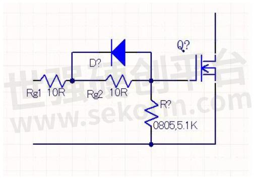
Fig.2 RG(on)=RG1+RG2,RG(off)=RG1
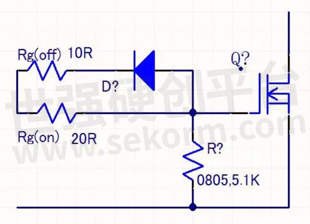
Fig.3 This design separates RG(on) from RG(off) for easy adjustment
3. For medium-power power supply (300W to 1500K), the drive design of the MOS tube not only needs to separate the open resistor and the off resistor but also needs to process the drive Miller platform. In general, a set of RC circuits will be added between the GS of the MOS tube to adjust the oscillation in the MILLER platform of the MOS tube by adjusting RC parameters. The design method is as follows:
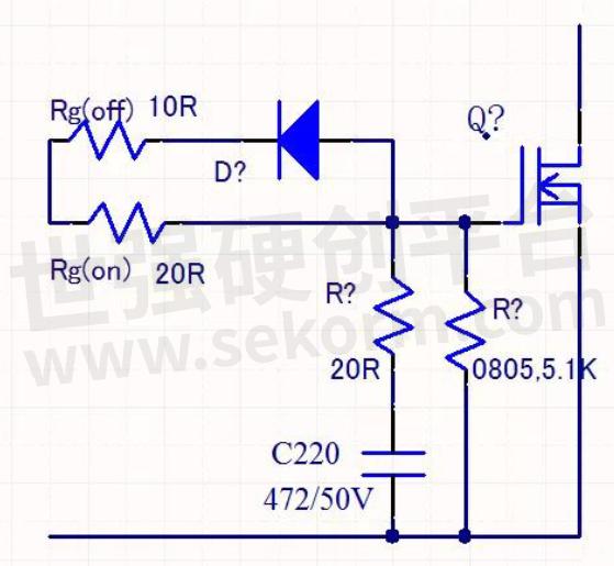
Fig.4
The parameter design should be based on the final debugging decision of the design circuit and MOS tube selection
4. It is particularly important for the drive design of MOS tubes for power supply with medium upper power or even high power (1200W to 5KW or even 10KW). At this time, the drive design has a great relationship with many aspects, including MOS tube selection, parasitic parameter differences between different manufacturers, power routing design, driver selection and design, drive loop design, and so on. Generally, MOS tube drive design has the following several design ideas. The main purpose is to suppress the oscillation and reduce the loop between THE GS of the MOS tube. The design method is as follows:
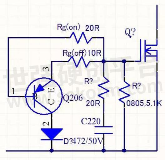
Fig.5
The triode is used to pull G class to S class directly when the drive is turned off.
The drive-off circuit is reduced and the drive anti-jamming ability is enhanced.

Fig.6
NMOS is used to pull the G class to the S class directly when the driver is turned off.
The drive off circuit is reduced and the drive anti-jamming ability is enhanced.

Fig.7
The triode is used to pull G class to S class directly when the drive is turned off. The drive off circuit is reduced and the drive anti-jamming ability is enhanced. At the same time the GS resistor series diode further enhances the anti-interference ability of the drive circuit.
5. The same is true in the design of the driver. The interference of the power loop must be reduced or even avoided. The specific design method is as follows:
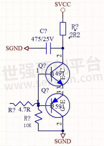
Fig.8
The totem pole is adopted as the driver, which is suitable for small and medium power products with low cost and strict requirements on cost.
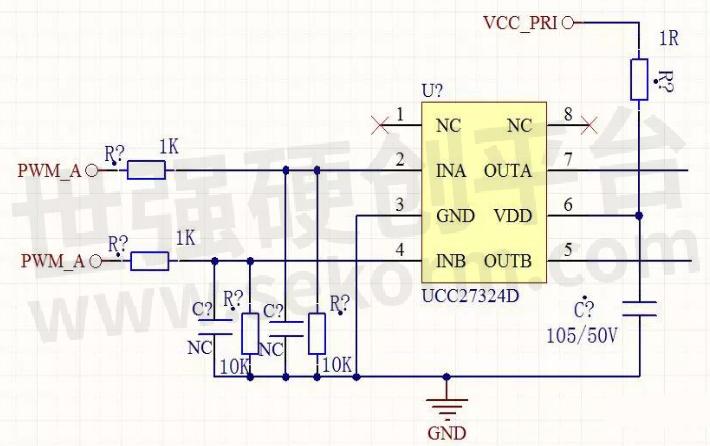
Fig.9
The drive IC is used as the driver to drive MOS or drive transformer, which is suitable for the design of large power and long drive circuits. The input end of the signal is added with pull-down resistance and RC filter to further process the IC input signal to ensure the signal is clean and enhance the anti-interference ability.
- |
- +1 赞 0
- 收藏
- 评论 0
本文由三年不鸣转载自HI-SEMICON News,原文标题为:The drive circuit design of MOS tube,本站所有转载文章系出于传递更多信息之目的,且明确注明来源,不希望被转载的媒体或个人可与我们联系,我们将立即进行删除处理。
相关推荐

MOS Switch Tube Selection and Principle Application
When the input voltage UI changes from high to low and the MOS tube changes from the on-off state to the cut-off state, the power UDD charges the stray capacitance CL via RD, charging time constant 1=RDCL, so the output voltage UO must pass a certain delay to change from the low level to the high level.

【经验】几种MOS管防反接防过压电路解析
关于MOS管防反接防过压电路您有了解吗?本文HI-SEMICON将为您介绍几种MOS管防反接防过压电路。当电源正确接入时。电流的流向是从V到负载,在通过NMOS到GND。刚上电时因为NMOS管的体二极管存在,地回路通过体二极管接通。

Switching Power Supply MOS Tube Loss
Switch Mode Power Supply, also known as switched Power Supply, switching converter, is a high-frequency Power conversion device, is a kind of Power Supply. Its function is to convert a potential voltage through different forms of architecture to the voltage or current required by the client. Switching power supplies convert voltages and currents between the inputs, which are mostly AC (such as mains power) or DC power, and the outputs, which are mostly devices requiring DC power, such as personal computers.

Why Can AO8822 Dual Nmos Tube Be Widely Used in Home Appliances, Leds and Other Products?
AO8822 products mainly play the role of switching and current and voltage regulation in the circuit. For example, in the motor driving circuit, the characteristics of AO8822 are suitable for various motor driving scenarios, including switching power supply products. Its extremely low on-resistance and high reliability help switching power supply products reduce energy loss and improve overall system efficiency.

Miller Effect on MOS Tube Switches
The gate drive process of MOSFET can be simply understood as the charging and discharging process of the input capacitance (mainly CGS of the gate source capacitance) of the MOSFET. When THE CGS reaches the threshold voltage, MOSFET will enter the opening state.

Application of Discrete Devices in Electric Shaver
HottechOne of the electric products commonly used by men is the electric shaver. Its working principle is to cut the beard by cutting the blade with a motor, usually with a rotary or reciprocating mechanism. Electric shaver is generally composed of power supply system, motor drive system, cutter head and cleaning system. In this issue, Hottech will mainly explain to you which device products are specifically used in boards such as power supply and motor drive.

【经验】防反接电路、电平转换电路、锁相电路中的MOS管电路分析
只要我们了解MOS管的特征参数,遇到MOS管电路,再也不会被电路分析难倒了。对于MOS管电路功能,HI-SEMICON还有一些小技巧分享给大家,比如针对防反接电路、逻辑电平转换电路、锁相电路,大家在用的时候可以手到擒来!
EASii IC 集成电路产品选型指南
X-REL Semiconductor Introduction Part Naming and Marking Codes POWER MANAGEMENT CLOCK & TIMING DISCRETES LOGIC INTERFACING & TRANSCEIVERS PACKAGE OUTLINES
EASII IC - SHUNT REGULATORS,N-CHANNEL POWER MOSFETS,PWM控制器,VERSATILE TIMER,FLEXIBLE FLOATING DRIVER,正串联稳压器,负串联稳压器,LOW-SIDE N-CHANNEL POWER MOSFET,FLEXIBLE POWER N-CHANNEL MOSFETS,N通道功率MOSFET,SMALL SIGNAL MOSFETS,POSITIVE-EDGE-TRIGGERED D-TYPE FLIP-FLOPS,“431”并联稳压器,PWM CONTROLLER,HIGH RELIABILITY AND HIGH TEMPERATURE INTEGRATED CIRCUITS,EDGE-TRIGGERED D FLIP-FLOP,POSITIVE SERIES VOLTAGE REGULATOR,SIC SCHOTTKY DIODE,ISOLATED TWO CHANNELS TRANSCEIVERS,TIMERS,高温80V低压侧N沟道功率MOSFET,HIGH INPUT VOLTAGE, 2A POSITIVE LDO REGULATOR,BUCK DC/DC,正负精密稳压器,传真机,晶体管,POWER GATE DRIVER,高可靠性高温集成电路,GENERAL PURPOSE DIODES,BUCK DC/DC,DIODE,FLOATING DRIVER,CLOCK,SIC SCHOTTKY DIODE,可重构逻辑门,灵活的浮动驱动器,浮动驱动器,BIDIRECTIONAL LEVEL TRANSLATORS,“431” SHUNT VOLTAGE REGULATOR,2TX/RX隔离数据收发器,PROGRAMMABLE SHUNT REGULATOR,降压直流/直流,HIGHLY STABLE, SMALL FOOTPRINT AND VERSATILE TIMERS,ISOLATED INTELLIGENT GATE DRIVER,NEGATIVE SERIES VOLTAGE REGULATOR,PWM CONTROLLER,分路调节器,时钟,HIGH-TEMPERATURE, HIGH RELIABILITY INTELLIGENT POWER TRANSISTOR DRIVER,SMALL-SIGNAL N- CHANNEL MOSFETS,边沿触发D触发器,SMALL FOOTPRINT PWM CONTROLLERS,低端N沟道功率MOSFET,高度稳定、小尺寸和多功能定时器,HIGH-TEMPERATURE 80V LOW-SIDE N-CHANNEL POWER MOSFET,N-CHANNEL POWER MOSFET,小信号P沟道MOSFET,高温、高可靠性智能功率晶体管驱动器,LOW-POWER VOLTAGE REGULATORS,小基底面PWM控制器,DISCRETES,HIGH-TEMPERATURE, HIGH RELIABILITY POWER TRANSISTOR DRIVER,TRANSISTOR,LDO REGULATOR,LOW-DROPOUT VOLTAGE REGULATOR,SMALL-SIGNAL P-CHANNEL MOSFETS,POSITIVE SERIES VOLTAGE REGULATOR,PROGRAMMABLE SHUNT REGULATOR,PMOS,多功能定时器,GATE DRIVER,高温双通道隔离数据收发器,计时器,高输入电压、2A正LDO稳压器,P沟道功率MOSFET,SMALL-SIGNAL P- AND N-CHANNEL MOSFETS,POSITIVE AND NEGATIVE PRECISION REGULATORS,VERSATILE TIMER,CRYSTAL OSCILLATOR DRIVER,通用二极管,FLOATING DRIVER,CRYSTAL OSCILLATOR DRIVER,BIDIRECTIONAL LEVEL TRANSLATORS,POWER GATE DRIVER,2TX/RX ISOLATED DATA TRANSCEIVER,4H-SIC结势垒肖特基二极管,可编程分流调节器,INTELLIGENT GATE DRIVER,LOW-DROPOUT VOLTAGE REGULATOR,隔离式双通道收发器,EDGE-TRIGGERED D FLIP-FLOP,ISOLATED TWO CHANNEL TRANSCEIVER,隔离式智能栅极驱动器,正边沿触发D型触发器,低压差稳压器,INTELLIGENT GATE DRIVER,高温、高可靠性隔离式功率晶体管驱动器,N沟道功率MOSFET,NEGATIVE SERIES VOLTAGE REGULATOR,闸门驱动器,NMOS,HIGH INPUT VOLTAGE 2A POSITIVE LDO REGULATOR,SMALL-SIGNAL P- CHANNEL MOSFETS,低功率稳压器,4H-SIC JUNCTION BARRIER SCHOTTKY DIODE,高温、高可靠性功率晶体管驱动器,P-CHANNEL POWER MOSFETS,N-CHANNEL POWER MOSFET,灵活的功率N沟道MOSFET,SMALL FOOTPRINT HIGH-TEMPERATURE, EXTENDED LIFETIME CRYSTAL OSCILLATOR DRIVERS,HIGH-TEMPERATURE DUAL-CHANNEL ISOLATED DATA TRANSCEIVER,GENERAL PURPOSE DIODES,SMALL-SIGNA N-CHANNEL MOSFETS,多功能逻辑门,HIGH-TEMPERATURE, HIGH RELIABILITY ISOLATED POWER TRANSISTOR DRIVER,小基底面、高温、长寿命晶体振荡器驱动器,P-CHANNEL POWER MOSFETS,高输入电压2A正LDO稳压器,SIC肖特基二极管,ISOLATED INTELLIGENT GATE DRIVER,双向电平转换器,小信号N沟道MOSFET,N-CHANNEL POWER MOSFETS,分立器件,功率门驱动器,TRANCEIVERS,RECONFIGURABLE LOGIC GATES,小信号P沟道和N沟道MOSFET,智能栅极驱动器,MULTI-FUNCTION LOGIC GATES,小信号MOSFET,晶体振荡器驱动器,二极管,XTR30018-,XTR1N0450-,XER2N0525,XTR60012-,XER2N0525-,XTR70022C-,XTR2601X,XTR65X FAMILY,XTR431,XTR75035-,XTR70022K-,XTR40010-,XTR25411-,XTR2N0307-,XTR2N0525-,XTR75011-,XTR30011-S,XTR20412A,XTR20412B,XTR1N0815,XTR30010-,XTR30021,XTR2N0807,XTR1N0415,XTR50011-,XTR5417X,XTR5001X FAMILY,XTR7503X,XTR50012,XTR70022B-,XTR2N0425,XTR50015,XTR SERIES,XTR30017-,XTR50014,XTR2N0825,XTR2N0307,XTR541G74-,XTRNNNNNP,XTR70022J-,XTR2N03XX,XTR2N0807-,XTR2041X,XTR655,XTR1N04XX,XTR70011-,XTR40011-,XTR1K1210-,XTR30021-,XTR7501X FAMILY,XTR3001X FAMILY,XTR7002X FAMILY,XTR2081X,XTR1N08XX,XTR2N0350-,XTR54175-,XTR7503X FAMILY,XTR30016-,XTR70022A-,XTR70022I-,XTR2N0350,XTR2081X FAMILY,XTR6001X FAMILY,XER30019-,XTR40012-,XTR20811-,XTR70022R-,XTR2N0325-,XTR4001X,XTR54175,XTR2N0450-,XTR50011,XTR2N0525,XTR30015-,XTR2602X,XTR2N08XX,XTR70022H-,XTR6001X,XTR75014-,XTR1K1210,XTR2N04XX,XTR70022Q-,XTR1N0815-,XTR2N0825-,XTR70025-,XTR655-,XTR75030-,XTR50010-,XTR3002X FAMILY,XTR7001X FAMILY,XTR30014-,XTR541G74,XTR70022G-,XTR1N0850-,XTR2N0450,XTR20412B-,XTR25020,XTR25011-,XTR75015-,XTR2N0850,XTR26020-,XTR70022P-,XTR75031-,XTR1N0850,XTR54000 FAMILY,XTR70020-,XTR54170-,XTR1N0450,XTR431-,XTR70022F-,XTR20412A-,XTR25010-,XTR2N05XX,XTR70022N-,XTR26021-,XTR70022O-,XTR70015-,XER30019,XTR541G7X,XTR3001X,XTR2502X,XTR2541X FAMILY,XTR70022E-,XTR2N0550,XTR650-,XTR25021-,XTR70022M-,XTR70010-,XTR,XTR7002X,XTR2541X,XTR2N0850-,XTR2N0X07,XTR7501X,XTR2N0325,XTR70022D-,XTR60011-,XTR3002X,XTR2501X,XTR5001X,XTRNNNNN,XTR651-,XTR1N0415-,XTR20411A-,XTR70022L-,XTR70021-,XTR75010-,XTR20812,XTR5417X FAMILY,XTR20811,XTR75034-,XTR65X,XTR7001X,XTR20412,XTR2N0425-,XTR20411,XTR50014-,XTR54000,XTR30011-,XTR2N0550-,XTR54000-,电机控制,ENERGY CONVERSION,UNINTERRUPTIBLE POWER SUPPLIES,IPM,CURRENT SOURCES,INTELLIGENT POWER MODULES,DC/DC CONVERTERS,DC/DC转换器,PFC,IPS,AUTOMOTIVE,POWER CONVERTERS,时钟产生,不间断电源,智能功率模块,功率转换器,UPS,不断电系统,POWER FACTOR CORRECTION,TIME-BASE GENERATOR,电桥激励,CABLE- POWERED APPLICATIONS,电缆供电应用,切换控制,SWITCHED MODE POWER SUPPLIES,PWM,MOTOR CONTROL,反馈网络,HIGH-EFFICIENCY REGULATED POWER SUPPLIES,PULSE WIDTH MODULATION,当前来源,电源管理,电压监测器,氮化镓驱动,VOLTAGE BLOCKING,A/D转换器,太阳的,接地开关,电池供电应用,切换应用,高效率稳压电源,POWER MANAGEMENT,POWER SWITCHING,VOLTAGE MONITORS,PPM,POWER SUPPLIES,MOSFET驱动,ISOLATED POWER INVERTERS,SWITCHING CONTROL,D/A转换器,时基发生器,电机驱动,SOLAR,信号切换,SIGNAL AMPLIFICATION,AERONAUTICS,功率转换,LINEAR RAMP GENERATOR,功率因数转换,ISOLATED GATE DRIVE,电平转换数据传输,POWER FACTOR CONVERSION,负载点电源转换器,精密定时,BRIDGE EXCITATION,航空,低压侧开关,SENSOR INTERFACING,CABLE-POWERED APPLICATIONS,晶体震荡器,汽车,电源切换,INTELLIGENT POWER SWITCHES,PWM控制,CRYSTAL OSCILLATORS,GAN DRIVING,发电,D/A CONVERTERS,RELIABILITY-CRITICAL,DC-DC CONVERTERS,AEROSPACE,隔离电源逆变器,线性斜坡发生器,SWITCHED-MODE POWER SUPPLIES,传感器接口,LOW SIDE SWITCHES,POWER SUPPLY,PRECISION TIMING,FEEDBACK NETWORKS,LEVEL SHIFTING,开关模式电源,LEVEL SHIFTED DATA TRANSMISSION,GROUND-CONNECTED SWITCHES,MOSFET DRIVING,MOTOR DRIVE,水平移动,POINT-OF-LOAD POWER CONVERTERS,ISOLATED POWER INVERTERS.,CLOCK GENERATION,GENERAL RECTIFICATION,电压闭锁,POWER GENERATION,ISOLATED SENSOR INTERFACES,PWM CONTROL,PULSE POSITION MODULATION,功率逆变器,伊普斯,能量转换,开关电源,SIGNAL SWITCHING,航空航天,信号放大,POWER CONVERSION,电动机驱动,隔离栅驱动,POWER INVERTERS,BATTERY-POWERED APPLICATIONS,A/D CONVERTERS,VOLTAGE CLAMPING,SWITCHING POWER SUPPLIES,WITCHING APPLICATIONS,DC-DC转换器,DOWN-HOLE,MOTOR DRIVES,MOTOR DRIVES,电压钳位,浮接开关,智能电源开关,POWER CONVERTERS,智能电源模块,功率因素矫正,全氟化碳,电源,FLOATING-CONNECTED SWITCHES,全面整改,SMPS

PNP Transistor TIP32A Can be Used in Audio Amplifier, Motor Driver and Power Supply
Hottech’s medium and high power amplifier transistor TIP32A has the advantages of high power handling capacity, high withstand voltage capacity, strong amplification performance, high temperature working capacity, good heat dissipation performance, stable physical and chemical properties, strong stability and reliability, and wide application range.

Details of MOS tube packaging
After the MOS tube chip is made, a shell is needed to be added to the MOS tube chip, which is the MOS tube package. The package housing mainly plays the role of support, protection and cooling, and also provides electrical connection and isolation for the chip, so as to form a complete circuit between MOS tube devices and other components. Different packaging, different design, MOS tube specifications, size, various electrical parameters, etc. will be different, and they can play a different role in the circuit will be different.

High Voltage MOS/IGBT Short Circuit Protection Circuit
When there is a short circuit in the circuit, the current flowing through MOS is very large, and the voltage drop generated at both ends of the S-pole resistance causes the triode to enter the conduction from the cut-off to the conduction (of course, the conduction to the specific degree depends on the transconductance of MOS). Therefore, there is a voltage drop on the driving resistance and MOS enters the amplifier. At this time, the high voltage will not carry out strong current discharge through MOS, so the chip will not have the possibility of local overheating.

HUA XUAN YANG ELECTRONIC Provides A Power Device Solution Tailored for In Car Wireless Mobile Phone Chargers
HUA XUAN YANG ELECTRONIC power device solution for car mounted wireless mobile phone chargers integrates efficient driving of MOS transistors, precise regulation of transistors, and pure power supply of LDO, optimizing charging performance in all aspects, providing car owners with a safe, fast, and worry free wireless charging experience.

MOS Tube Knowledge, Must Read!
According to the size of PCB board, select the appropriate PMOS tube size, in the case of limited on-board area, choose the small package as far as possible; As far as possible to select common packaging, to prepare for the subsequent selection of appropriate replacement material.

MOS Tube H Bridge Motor Drive Circuit Diagram
H bridge is a typical DC motor control circuit, because its circuit shape resembles the letter H, so it is named “H bridge“. Four audions constitute the four vertical legs of H, and the motor is the horizontal bar in H (note: the figure is only a schematic diagram, rather than a complete circuit diagram, in which the driving circuit of the audion is not drawn).

HKT NMOS Tube HKTG50N03 Can Be Used in BMS, LED Driving, Fast Charging and Power Supply
With the increasing market demand for high current and high efficiency switches, HKTG50N03, a discrete device with high current capability, has many uses. HKTG50N03 product is a stable, safe and powerful MOS product, and its switching ability, voltage regulation ability, efficient working ability and stable and reliable current control ability are promising.

电子商城


现货市场

服务
定制液冷板尺寸5mm*5mm~3m*1.8m,厚度2mm-100mm,单相液冷板散热能力最高300W/cm²。
最小起订量: 1片 提交需求>
授权代理品牌:集成电路


授权代理品牌:分立元件


授权代理品牌:接插件及结构件


授权代理品牌:部件、组件及配件


授权代理品牌:电源及模块


授权代理品牌:电子材料


授权代理品牌:仪器仪表及测试配组件


授权代理品牌:电工工具及材料


授权代理品牌:机械电子元件


授权代理品牌:加工与定制


登录 | 立即注册
提交评论