Solve the mystery of MOS tube damage


Today, we share about solving the mystery of MOS tube damage.
1. Avalanche damage
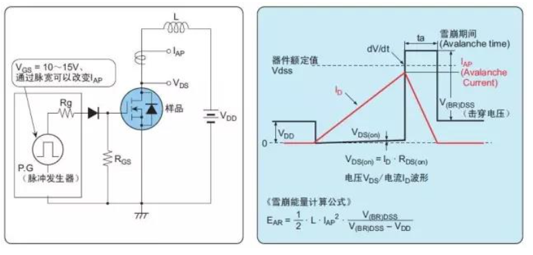
Failure occurs when a breakdown voltage, V(BR)DSS (depending on the breakdown current), is applied between the drain and source electrodes beyond the rated VDSS of the device and a certain amount of energy. Avalanche failure can be caused by a back sweep voltage generated when a dielectric-loaded switch is running off, or by a mode in which the peak voltage generated by the leakage inductance exceeds the power MOSFET's drain-rated withstand voltage and enters the breakdown zone.
Typical circuit:

Fig.1
2. Device heating damage
Caused by a fever outside a safe area. The causes of heating can be divided into dc power and transient power. Dc power cause: Heating caused by loss of applied DC power
RDS(on) loss of on-off resistance (RDS(on) increases at high temperature, resulting in certain current current and increased power consumption)
Losses caused by leakage current IDSS (very small compared with other losses)
Cause of transient power: plus single trigger pulse
Load short circuit
Switch loss (on, off) * (related to temperature and operating frequency)
TRR losses of built-in diodes (short circuit losses of upper and lower bridge arms) (related to temperature and operating frequency)
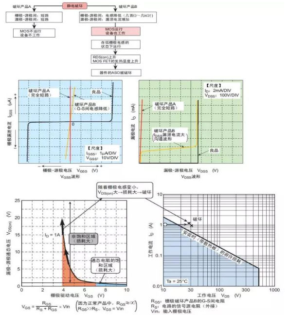
The overcurrent caused by the load short circuit does not occur during the normal operation of the device, causing instantaneous local heat and resulting in damage. In addition, when the chip cannot dissipate heat normally due to heat mismatch or the switch frequency is too high, the continuous heating will cause the temperature beyond the channel temperature and lead to the destruction of thermal breakdown.

Fig.2
3. Internal diode damage
When the parasitic diode formed between the DS ends runs, this mode of diode failure is caused by the parasitic bipolar transistor running at MOSFET power at Flyback.

Fig.3
4. Damage caused by parasitic oscillations
This failure mode is particularly prone to occur in parallel.
Gate parasitic oscillation occurs when grid resistance is not inserted in parallel power MOS FET but connected directly. This parasitic oscillation occurs on a resonant circuit formed by gD-drain capacitor CGD(CRSS) and gate pin inductance Lg when the drain-source voltage is switched on and off repeatedly at high speed. When resonance conditions (omega = 1 L/C omega) were found, in the grid - the source electrode and is far greater than the vibration of the driving voltage VGS (in) voltage, due to beyond grid-rated voltage source electrode grid, or switching, disconnect the drain-source electrode voltage vibration voltage through the grid - drain capacitance CGD and VGS waveform overlap lead to positive feedback, so may be caused by misoperation oscillation.

Fig.4
5. Grid surge and electrostatic failure
There are mainly failures caused by voltage surge and static electricity between the gate and the source, namely gate overvoltage failure and gate failure caused by static electricity in the on-charge state at both ends of GS (including installation and electrification of measuring equipment).

Fig.5
- |
- +1 赞 0
- 收藏
- 评论 0
本文由三年不鸣转载自HI-SEMICON News,原文标题为:Solve the mystery of MOS tube damage,本站所有转载文章系出于传递更多信息之目的,且明确注明来源,不希望被转载的媒体或个人可与我们联系,我们将立即进行删除处理。
相关推荐
MOS Switch Tube Selection and Principle Application
When the input voltage UI changes from high to low and the MOS tube changes from the on-off state to the cut-off state, the power UDD charges the stray capacitance CL via RD, charging time constant 1=RDCL, so the output voltage UO must pass a certain delay to change from the low level to the high level.
MOS Tube Anti-overvoltage Circuit
When the power is properly connected. The current flows from VIN to the load, through NMOS to GND. At the beginning of power on, because the body diode of the NMOS tube exists, the ground circuit is connected through the body diode. Later, because the VGS is greater than the threshold voltage of VGSTH, the MOS tube conducts.
Switching Power Supply MOS Tube Loss
Switch Mode Power Supply, also known as switched Power Supply, switching converter, is a high-frequency Power conversion device, is a kind of Power Supply. Its function is to convert a potential voltage through different forms of architecture to the voltage or current required by the client. Switching power supplies convert voltages and currents between the inputs, which are mostly AC (such as mains power) or DC power, and the outputs, which are mostly devices requiring DC power, such as personal computers.
Miller Effect on MOS Tube Switches
The gate drive process of MOSFET can be simply understood as the charging and discharging process of the input capacitance (mainly CGS of the gate source capacitance) of the MOSFET. When THE CGS reaches the threshold voltage, MOSFET will enter the opening state.
MOS Tube Knowledge, Must Read!
According to the size of PCB board, select the appropriate PMOS tube size, in the case of limited on-board area, choose the small package as far as possible; As far as possible to select common packaging, to prepare for the subsequent selection of appropriate replacement material.
MOS Tube and Simple CMOS Logic Level Circuit
Take n-type tube as an example, and the 2 ends are the control ends, which are called “gate“. The 3-terminal is usually grounded and is referred to as the “source“; The source voltage is denoted as VSS, the positive voltage at the end is called “drain“, and the drain voltage is denoted as VDD. To enable terminal 1 and terminal 3 to conduct, the level on gate 2 must be increased.
MOS Tube H Bridge Motor Drive Circuit Diagram
H bridge is a typical DC motor control circuit, because its circuit shape resembles the letter H, so it is named “H bridge“. Four audions constitute the four vertical legs of H, and the motor is the horizontal bar in H (note: the figure is only a schematic diagram, rather than a complete circuit diagram, in which the driving circuit of the audion is not drawn).
MOS tube structure principle
Structure and symbol (take n-channel enhanced type as an example) -- Two high-concentration N-type areas are diffused on a low-concentration P-type silicon as drain and source, the semiconductor surface is covered with a silicon dioxide insulation layer and an electrode is drawn as a gate.
Is It Always Difficult to Use and Replace MOS Tubes for Multimeter Tests?
MOS tube has always been one of the topics that engineers are keen to discuss, so we have sorted out the common and uncommon knowledge of MOS tube, hoping to be of some help to engineers. Now let‘s talk about the MOS tube, a very important component. Antistatic protectionAlthough the MOS tube has internal protection measures, we should also operate by the anti-static operation rules, which qualified maintenance personnel should have.
Details of MOS tube packaging
After the MOS tube chip is made, a shell is needed to be added to the MOS tube chip, which is the MOS tube package. The package housing mainly plays the role of support, protection and cooling, and also provides electrical connection and isolation for the chip, so as to form a complete circuit between MOS tube devices and other components. Different packaging, different design, MOS tube specifications, size, various electrical parameters, etc. will be different, and they can play a different role in the circuit will be different.
Hardware Necessary Skills, MOS Tube Composed of Basic Gate Logic Circuit
As a hardware engineer, you can‘t help but understand chips. In order to understand the chip, the basic logic circuits composed of MOS tubes must be memorized so as to be able to understand the chip block diagram more proficiently. The field-effect Transistor provides a variety of gate circuits that can be visualized in a variety of combinations or visuals that, as the description in the beginning, may be the basis of a modern IC.
Explain in Detail the Cause of MOS Tube Heating
For power supply design or driving circuit, it is inevitable to use field effect tube, which is often called MOS tube. There are many kinds of MOS tubes and they have many functions. To do the use of power or drive, of course, is to use its switching action.Regardless of N type or P type MOS tube, the operating principle is essentially the same. MOS transistors control the drain current at the output end by applying voltage to the gate at the input end. MOS tube is a voltage control device.
Experience sharing of classical MOS transistor level conversion circuit
Level switch in the circuit design is very common, because of circuit design, most of the time just like in the building blocks of the circuit module, and the circuit module, patchwork together is a electronic products. However, the voltage domain is often inconsistent between modules, so the level conversion circuit is used for the communication between modules.
Why are MOS tubes broken down by static electricity,and what should we do about it?
MOS tube a ESD sensitive devices, its input resistance is very high, and the gate electrode capacitance is very small, so vulnerable to external electromagnetic or electrostatic induction and charged (a small amount of charge on the interelectrode capacitance can form a very high voltage (think U = Q/C) will be pipe damage, and because of the strong electrostatic situation difficult to charge and discharge to electrostatic breakdown.
MOS Tube Drive Circuit Summary - Detailed Design of Various Switching Power Supply MOS Tube Drive Circuit
When using MOS tube drive circuit to design switch power supply or motor drive circuit, most people will consider MOS conduction resistance, maximum voltage, maximum current, etc., and many people only consider these factors. Such circuits may work, but they are not excellent and are not allowed as a formal product design.
电子商城
现货市场
服务
可根据用户的MOSFET管进行参数检测出具报告,静态参数最大电压:7500V、检测最大电流6000A;动态参数最大电压:3300V、检测最大电流:4500A。该测试标准满足GB、IEC及行业标准等,具备可靠性评估及老化实验能力。
实验室地址: 西安 提交需求>
定制液冷板尺寸5mm*5mm~3m*1.8m,厚度2mm-100mm,单相液冷板散热能力最高300W/cm²。
最小起订量: 1片 提交需求>


登录 | 立即注册
提交评论