Switching Power Supply MOS Tube Loss


Switch Mode Power Supply, also known as a switched Power Supply, or switching converter, is a high-frequency Power conversion device, is a kind of Power Supply. Its function is to convert a potential voltage through different forms of architecture to the voltage or current required by the client. Switching power supplies convert voltages and currents between the inputs, which are mostly AC (such as mains power) or DC power, and the outputs, which are mostly devices requiring DC power, such as personal computers.
Switch losses include conduction losses and cut-off losses. Conduction loss refers to the power loss generated when the power tube is cut off to conduction. Cut-off loss refers to the power loss generated when the power tube is switched on to cut-off. Switching losses, which include turn-on Loss and turn-off Loss, are often discussed in Hard- and soft-switching. The so-called turn-on Loss refers to that when a non-ideal switching tube is turned on, the voltage of the switching tube does not immediately drop to zero but has a time of decline. Meanwhile, its current does not immediately rise to the load current but also has a time of rise. During this period, the current and voltage of the switching tube have an overlapping area, resulting in a loss, which is the switching loss. By using this analogy, we can get the cause of the turn-off loss, which will not be repeated here. Switching loss another meaning is that in the switching power supply, the parasitic capacitor needs to be charged and discharged when the large MOS tube is switched on and off, which will also cause losses.
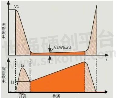
Fig.1
Several basic principles of MOS design and selection
1. Voltage stress
In the application of a power supply circuit, the choice of drain-source voltage VDS is usually considered first. The basic principle on this is that the maximum peak voltage between the drain terminals in the actual MOSFET operating environment should not be greater than 90% of the nominal leakage source breakdown voltage in the device specification.
That is:
VDS_peak ≤ 90% * V(BR)DSS
Note: In general, V(BR)DSS has a positive temperature coefficient. Therefore, the V(BR)DSS value at the lowest operating temperature should be taken as a reference.
2. Drain current
Then consider the drain current selection. The basic principle is that the maximum periodic drain current in the actual MOSFET working environment should not be greater than 90% of the nominal maximum drain-source current in the specification. The peak value of the drain pulse current shall not be greater than 90% of the nominal peak value of the drain pulse current in the specification, namely:
ID_max ≤ 90% * ID
ID_pulse ≤ 90% * ID P
Note: Generally, ID_max and ID_pulse have negative temperature coefficients, so the ID_max and ID_pulse values under maximum junction temperature should be taken as references. The selection of this parameter is highly uncertain -- it is mainly due to the mutual influence of the working environment, heat dissipation technology, and other parameters of the device (such as conduction resistance, thermal resistance, etc.). The final decision is based on the node temperature (i.e., the "dissipated power constraint" in Article 6). As a rule of thumb, the ID in the specification will be several times larger than the actual maximum operating current in practical applications due to the limitations of dissipation power and temperature rise. In the primary calculation period, this parameter must be adjusted continuously according to the dissipation power constraint in Article 6 below. ID = (3~5)*ID_max is recommended.
3. Driving requirements
MOSFEF's driving requirement is determined by its gate total charge capacity (QG) parameter. In the case of meeting other parameter requirements, try to choose QG small for the design of the drive circuit. The drive voltage is selected to keep Ron as small as possible while keeping it away from the maximum gate-source voltage (VGSS) (generally using the recommended values in the device specification).
4. Loss and heat dissipation
A small Ron value is conducive to reducing the loss during the conduction period, while a small RTH value can reduce the temperature difference (under the same condition of dissipated power), so it is conducive to heat dissipation.
5. Preliminary calculation of power loss
MOSFET loss calculation mainly includes the following eight parts:
PD = Pon + Poff + Poff_on + Pon_off + Pds + Pgs+Pd_f+Pd_recover
The detailed calculation formula shall be determined according to the specific circuit and working conditions. For example, in synchronous rectifier applications, the loss during the forward guide of the internal diode and the reverse recovery loss at the turn cut-off are also taken into account. The loss calculation can be referred to in the "8 Components of MOS Tube Losses" section below.
6. Dissipation power constraint
Device steady-state loss power PD, Max should be considered based on the maximum operating junction temperature limit of the device. If the operating environment temperature of the device can be known in advance, the maximum dissipated power can be estimated by the following method:
PD, Max ≤ (Tj, max-tamb)/R j-a
R j-A is the total thermal resistance between the node of the device and its working environment, including R junction-case, R case-sink, R sink-ambiance, etc. If there are insulating materials, thermal resistance shall also be taken into account.
MOS tube loss of 8 components
In the process of device design selection, it is necessary to carry out an advance calculation for MOSFET working process loss (the so-called advance calculation refers to the theoretical approximate calculation using the parameters provided in the device specification and the calculated value and expected waveform of the working circuit, in the case of failing to test each working waveform).
1. Conduction loss Pon
On loss is the loss caused by the voltage drop of the load current IDS(on)(t) on the on-resistance RDS(on) after MOSFET is fully switched on.
Calculation of conduction loss:
First, the function expression of IDS(on)(t) is calculated, and the effective value of IDS(on) RMS is calculated. Then, the resistance loss is calculated as follows:
Pon=IDS(on) RMS2 × RDS(on) × K × Don
Description:
The period used to calculate IDS(on) RMS is only the lead time Ton, not the entire work cycle Ts; RDS(on) varies with IDS(on)(t) values and device node temperatures, and the principle here is to look for RDS(on) values as close to the expected operating conditions as possible according to the specification (that is, multiplied by a temperature coefficient K provided by the specification).
2. Cut-off loss Poff
Cut-off loss refers to the loss caused by leakage current IDSS generated under the leak-source voltage VDS(OFF) stress after MOSFET is completely cut off.
Cut-off loss calculation:
Firstly, the leakage source voltage VDS(OFF) sustained by MOSFET is calculated. Then, the IDSS provided in the device specification is searched and calculated by the following formula:
Poff=VDS(off) × IDSS × (1-don)
Description:
IDSS varies according to VDS(off), and the value provided in the specification is a parameter in an approximate V(BR)DSS condition. If the calculated drain-source voltage VDS(off) is large enough to be close to V(BR)DSS, this value can be directly referenced; if very small, zero value is preferred, i.e., this value is ignored.
3. Opening process loss
Opening loss refers to the loss caused by the cross overlap between the decreasing drain-source voltage VDS(OFF_on)(T) and the increasing load current (i.e., drain-source current) IDS(OFF_on)(t) during MOSFET opening.
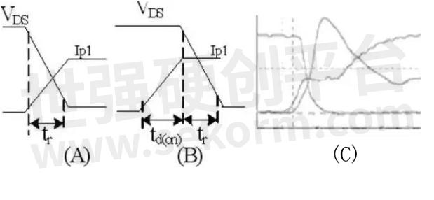
Fig.2
Calculation of opening process loss:
The cross waveform of the opening process VDS(OFF_on)(t) and IDS(OFF_on)(t) is shown in the figure above. VDS(OFF_end) before the start time, IDS(on_beginning) after the start time, Ip1 diagonally, and Tx overlap time between VDS(off_on)(t) and IDS(Off_on)(t) must be calculated or expected first. Then, it can be calculated by the following formula:
Poff_on = fs x ∫ Tx VDS (off_on) (t) * ID (off_on) (t) * dt
There are two main assumptions in the actual calculation -- figure (A) assumes that the initial decline of VDS(OFF_on)(t) occurs simultaneously with the gradual rise of ID(off_on)(t); Figure (B) assumes that the decline of VDS(off_on)(t) begins after ID(off_on)(t) rises to its maximum value. Figure (C) is the actual MOSFET test waveform in the FLYBACK architecture path, which is closer to the class (A) hypothesis. Two calculation formulas are extended for these two hypotheses:
Class (A) assumes Poff_on=1/6 × VDS(off_end) × Ip1 × tr × FS
Class (B) assumes Poff_on=1/2 × VDS(off_end) × Ip1 × (TD (on)+ TR) × FS
(B) Class assumptions can be calculated as values for the most egregious patterns.
Description:
In Figure (C), we can see the IDS(on_beginning)>>Ip1 after starting (the Ip1 parameter in the power supply is usually the initial value of excitation current). The exact value of the superimposed current crest is difficult to predict and depends on the circuit architecture and device parameters. For example, the actual current in FLYBACK would be Itotal=Idp1+Ia+Ib (Ia is the current value of the reverse recovery of the secondary rectifier diodes that influenza should return to the primary electrode -- that is, multiplied by the turn ratio, Ib is the current released by the parasitic capacitance between the layers of the primary side winding of the transformer as soon as the MOSFET switch is turned on). This hard-to-predict value is also one of the main reasons for this part of the calculation error.
4. Loss during turn-off
Turn-off loss. Refers to the loss caused by the crossover overlap between the gradually rising drain-source voltage VDS(on_off) (T) and the gradually falling drain-source current IDS(ON_off)(t) during MOSFET switching.
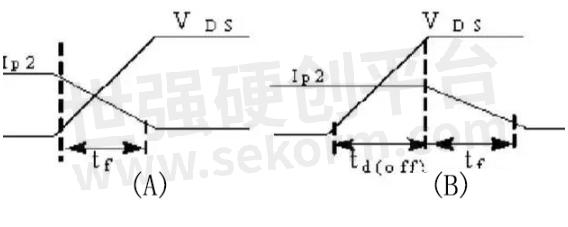
Fig.3
Calculation of loss in the turn-off process:
As shown in the figure above, the loss calculation principle and method of this part are similar to Poff_on. The drain-source voltage VDS(OFF_off) and load current IDS(on_end) before the turn-off should be calculated or expected first, as shown in Ip2, and the overlap time Tx between VDS(on_off) (T) and IDS(on_off)(t). Then, it can be calculated by the following formula:
Poff_on= FS × integral of Tx VDS(on_off) (t) × IDS(on_off)(t) × dt
In the actual calculation, two calculation formulas are extended for these two hypotheses:
Class (A) assumes Poff_on=1/6 × VDS(off_beginning) × Ip2 × TF × FS
Class Poff_on=1/2 × VDS(off_beginning) × Ip2 × (TD (off)+ TF) × FS
(B) Class assumptions can be calculated as values for the most egregious patterns.
5. Drive loss Pgs
Drive loss refers to the loss caused by the gate receiving the drive power for driving
Calculation of drive loss:
After the VGS of the driving power supply is determined, it can be calculated by the following formula:
Pgs= VGS × QG × fS
instructions:
QG is the total driving power, which can be found through the device specification.
6. Dissipation loss Pds of Coss capacitance
The discharge loss of the Coss capacitor refers to the discharge loss of the electric field energy stored in the MOS output capacitance Coss during the cut-off period on the drain-source pole.
Calculation of dissipation losses of Coss capacitors
The VDS before the start time must be calculated or anticipated and then calculated using the following formula:
Pds=1/2 × VDS(off_end)2 × Coss × FS
instructions:
Coss is MOSFET output capacitance, generally equal to CDS, this value can be found through the device specification.
7. Parasitic diode forward guide loss Pd_f
The forward guide loss of the parasitic diode in MOS refers to the loss caused by the forward voltage drop when the parasitic diode in MOS carries forward current.
Forward guide loss calculation of internal parasitic diode
In some applications where a parasitic diode is used to carry current (e.g. synchronous rectification), the loss of this part needs to be calculated. The formula is as follows:
PD_f = IF × VDF × Tx × f
Where: IF is the current carried by the diode, VDF is the diode positive guide pass-pressure drop, and TX is the time of the diode carrying current within a week.
instructions:
It varies depending on the junction temperature of the device and the current carried. The value can be as close as possible to the specification book according to the actual application environment.
8. Body parasitic diode reverse recovery loss Pd_recover
Reverse recovery loss of parasitic diode in MOS refers to the loss of reverse recovery caused by reverse pressure after the parasitic diode in MOS carries forward current.
In vivo, parasitic diode reverse recovery loss calculation
This loss principle and calculation method is the same as the reverse recovery loss of an ordinary diode. The formula is as follows:
PD_recover=VDR × QRR × FS
Wherein: VDR is diode reverse pressure drop, QRR is diode reverse power recovery, found in the specification provided by the device.
Methods to reduce MOS tube losses
On the one hand, it is necessary to make devices with ideal switching characteristics as much as possible, and on the other hand, it is necessary to make use of new circuit technology to change the waveform of the device switching period, such as transistor buffer circuit, resonant circuit, soft switch technology and so on.
(1) Transistor buffer circuit (i.e., additive absorption network technology)
The circuit technology was used in early power supply. Using this circuit, although the power loss is reduced, it is still not ideal.
Reduce the conduction loss in the transformer behind the secondary coil with saturated inductance, add the reverse recovery time fast diode, use the characteristics of the saturated inductance to hinder the current change, and limit the rate of current rise, so that the current and voltage waveform as small as possible overlap.
Reduce the cut-off loss plus R, C absorption network, and delay the transformer flyback voltage generation time, it is best to generate flyback voltage when the current is 0, at this time the power loss is 0. The circuit takes advantage of the characteristic that the capacitor voltage cannot be suddenly changed to delay the occurrence time of flyback voltage. To increase reliability, R and C can also be added to the power tube. However, this circuit has an obvious disadvantage: due to the presence of resistance, the absorption network is lost.
(2) Resonance circuit
The circuit only changes the instantaneous current waveform of the switch and does not change the current waveform of the conduction time. As long as the appropriate L and C are selected and combined with diode junction capacitance and transformer leakage inductance, the switching tube can be switched on or off when the voltage is 0. Therefore, using resonance technology can make the switch loss small.
(3) Soft switch technology
This circuit is in the full-bridge inverter circuit to add capacitance and diode. The diode plays a clamping role in the switching tube conduction, and forms a discharging circuit, discharging the current. Capacitance under the action of flyback voltage, the capacitor is charged, and the voltage cannot be suddenly increased, when the voltage is relatively high, the current has been 0.
- |
- +1 赞 0
- 收藏
- 评论 0
本文由三年不鸣转载自HI-SEMICON News,原文标题为:Switching power supply MOS tube loss,本站所有转载文章系出于传递更多信息之目的,且明确注明来源,不希望被转载的媒体或个人可与我们联系,我们将立即进行删除处理。
相关推荐

MOS Switch Tube Selection and Principle Application
When the input voltage UI changes from high to low and the MOS tube changes from the on-off state to the cut-off state, the power UDD charges the stray capacitance CL via RD, charging time constant 1=RDCL, so the output voltage UO must pass a certain delay to change from the low level to the high level.

Application of Discrete Devices in the Control Panel of 3D Printer
Many people may have heard of 3D printing, and now many products are printed by 3D printers. In this issue, Heketai will show you the working principle of the magical 3D printer and the components used in the control panel.

MOS Tube H Bridge Motor Drive Circuit Diagram
H bridge is a typical DC motor control circuit, because its circuit shape resembles the letter H, so it is named “H bridge“. Four audions constitute the four vertical legs of H, and the motor is the horizontal bar in H (note: the figure is only a schematic diagram, rather than a complete circuit diagram, in which the driving circuit of the audion is not drawn).

合科泰宣传册(HOTTECH CORPORATE BROCHURE)
目录- 公司简介 半导体生产流程及设备 电阻生产流程及设备 质控系统及检测设备 智能仓储 保护器件产品介绍 保护器件产品热销型号
型号- 15MQ040,US2DBF,RS2ABF,US2DF,M7L,DS28W,B0530WS,MM1Z6V2L,2SC4116,BZT52B7V5,US2DL,MJE170,SS120F,MMBT4401,S1DBF,DFLT15A,2SC4102,MM1Z4V7L,KTD1351,RHN1210,MMBT4403,BZX84C4V7W,DFLT5V0A,SM516,MMST2907A,SM518,7N65F,DS26W,RHN1206,DFLT14A,MMST2222A,2SA1213,BZV55B2V0,MUR120S,BZV55B2V2,US2BL,BZV55B2V4,US2BF,30BQ040,2SB1260,BZV55B2V7,SMAJ8.0A,MMBD4148A,2SA812,BZT52C7V5S,NCP1402SN33T,MMBD2835,DFLT13A,2SB1274,30BQ060,S15GL,4N80F,1117-1.5-223,LM4002,74HC4051,LM4001,5N60F,BZT52B9V1,LM4007,DS24W,15N10,RHN2512,LM4004,S2GBF,LM4003,DFLT12A,LM4006,LM4005,S15AL,BZT52C5V6S,8N80,BAS40-04,KSA1220A,MM1Z4V3L,2N5551K,DFLT11A,KTA968A,2SA673A,US2AL,BAT46WS,1N4448WS,US2AF,G1A,AO8808A,G1B,2SA844,G1D,G1G,2SA608,SS210F,BAS416,G1J,BZX84C6V2W,2SA1012,2SA1013,2SA1015,DFLT10A,SM513,TIP31A,TIP31C,SS220BF,DS22W,RI0805,BZV55B4V3,BD034,ES1GBF,BZV55B4V7,MUR140S,S15DL,ZVN3310F,TL432,US3GBF,TIP32A,TIP32B,NTR2101P,S15BL,TIP32C,ZXMP10A18,SI4466DY,4N60F,DFLT7V0A,74HC138,BAT720,S9018W,2SD1724,DS210W,BAV20WS,BZX84C2V4W,BAS20H,KTC2238,B5819W,P0080SA,S2ABF,SK32B-SK310B,BZX84C9V1,1SS400,RA022A,2N7002K,AO3480,BAV70W,JRC4558,RHA0805,MUR105S,BAT54S,SS215BF,RS1KBF,RA024A,BAS21C,BZT52C5V1S,US1GBF,BAT54H,B5818W,RLH1210,PZT4403,BAS21A,BAT54C,PZT4401,BAT54A,US2MF,1N5818W,DS212W,ES1EBF,US2JL,MBR220L,US2JF,BAS70-04,RI0603,US2B,RLH1206,US2A,AO4314,BZV55B6V2,TP4056,US2K,BD234,AO4310,US2J,10MQ100,BD236,AO4312,BZV55B6V8,US2G,BD238,BD237,BZX84C2V2W,RS2AL,US2D,RS2AF,US2M,7N60F,1N5817W,BZT52C3V9S,MB05S,US1B,MB05M,B0540W,US1A,1117-1.8-252,RAT0603,S3BBF,US1J,PXT8550,US1G,SK340LFL,US1D,MB05F,SS212F,US2KF,US1K,SMBJ5.0A,1117-1.8-223,US4D,BZX84C62W,2SD1762,US4B,US4A,US2JBF,BZX84C7V5,RHA0603,US4J,US4G,MM1Z27L,S1BBF,1N60,ES2DBF,ZMM3V0,US3D,BZX84C4V3W,US3B,US3A,1N65,ZMM3V6,US3K,RI01005,US3J,2SB772,US3G,RI0402,2SB776,MBRS540T3,RCQ2010,DMN13H750S,US3M,BZV55B10,ES1CBF,BZV55B12,MM1Z8V2L,BZV55B11,B5817W,BZT52C3V6S,BZV55B8V2,RS1MBF,BD437,BAT54W,BAS21S,DMN10H220L,RHR0805,NTC1206,S3DBF,US2GF,BZX84C2V7W,US2GL,BD683,BD440,BD442,ZVP0545,MM1Z6V8L,MM1Z22L,NTC0603,RHRT0603,1117-3.3-223,AO3407,AO3401,BAS70,AO3402,79L05,BZT52C27S,AO3403,AO3404,BZX84C5V6,79L08,B5819WS,79L09,79L06,AO3400,BZX84C5V1,RHA0402,RHN0805,RS2GF,RS2GL,DMNH10H028SCT,1N4001WS,74HC595D,MMSTA92,AO3419,SS24BF,RS1GBF,AO3415,RI0201,ES1JL,TI431,KBP301G,LT3465ES6,MM1Z24L,3N50F,S3AF,1N4001W,SMBJ7.0A,2SC1623,2SC2712,2SC2714,1N4001L,2SD882,ES1JF,US2KBF,2SD880,3N50,MMST4403,RABF210,1117-5.0,DL4001,DL4002,MMST4401,DL4003,DL4004,DL4005,KBP302G,DL4006,10MQ060,SMAJ14A,DL4007,MPSA56,1N4002W,SMCJ9.0A,ES2CBF,BZT52C2V4S,79L12,79L15,1N4002L,US1JBF,D882,S1KBF,KBP303G,SMAJ15A,NTC0402,1N4003W,1N4003L,ES1GF,BZX84C3V9,BZX84C3V6,BZX84C3V0,ES1GL,SMAJ12A,10N65F,S3BF,BZT52C22S,1N4004W,2SC1674,AO4308,KSA708,AO4304,1N4003WS,SS22BF,AO4306,BAS40,1N4004L,RS2BL,KEJ3055,AO4302,BC848W,SMAJ13A,RS2BF,BAV101,MM1Z20L,S1AF,BAV103,BAV102,1N4005W,US2MBF,KTC3265,RS2JBF,AO3423,S8050,PZTA94,KTA1276,PZTA92,8N60F,BZX84C68W,1N4005L,ES1EB,AO3421,B0520LW,BC847W,ES1EL,7N80F,SMAJ10A,DS215W,S3DF,LM358DR,1N4006W,ES2ABF,MMST5551,BZT52C24S,AO3435,1117-3.3-252,GL34A,1N4006L,RS2DL,ES1DB,2N3904,BZT52C2V0S,BC846W,GL34D,GL34B,ES1DF,RS2DF,ES1DL,S1MBF,SMAJ11A,BZX84C7V5W,MM1Z3V3L,ZVP2110,RAT2010,SMBJ9.0A,1N4007W,PZT2222A,2SC1008,GL34G,2SD2136,GL34J,ES1CB,1N4007L,SMAJ6.0A,ES1CF,P0720SA,A92,DMT10H010LCT,ES1CL,MMBTA56,BAV16W,MMBTA44,CJN5616,MMBTA42,S1BF,PZTA44,ZVP4525,PZTA42,5N60,SMCJ7.0A,1N4005WS,ES1BB,P0900SA,ES1BF,S3GF,ES1BL,BZT52B2V7,ES1C,2N7002,SMCJ14A,RS2DBF,ES1D,ES1E,ES1G,ES1J,PZTA56,2SC2314,PZT3906,PZT3904,BZT52B2V4,SK110L,SK82-SK810,1117-1.8,1117-1.5,ES1AB,KSB1151,S3JF,ES1AF,2SB1658,ES1AL,SS12F,ES2A,ES2B,ES2C,SMCJ15A,BZT52C20S,S1GBF,US3ABF,2SC1213,S1DF,NE555DT,SMBJ10A,MMBT5551,ES1A,ES1B,ES3E,ES3G,BAV19W,SMCJ12A,MMSTA42,ES3J,RS2KF,ES3K,US2BBF,ES3M,NTC0805,1117-2.5-223,78M12,BZT52B22,78M15,78M18,BZT52B24,1N4448W,BZT52B27,TL494DR,BAS70WS,ES4A,KBP304G,SMCJ11A,ES4B,RHN0603,ES4C,1117-1.5-252,SKI3L,B5817WS,BZT52B20,RI2012,ES2D,2SA1203,BZT52C9V1S,ES2E,SMCJ13A,ES2G,ULN2003DR,US1ABF,ES2J,2SA1201,B0520WS,RS2JF,PZT2907A,FDN338P,RLH1812,78M05,BZT52B33,78M06,BZT52B36,78M09,78M08,DFLT9V0A,BZT52B39,RS2JL,KBP305G,S1GF,MMBD4148W,ES3A,S3KF,ES3B,SS8050,BZT52B30,ES3C,SKI2L,ES3D,RS2MF,BZT52B4V3,BZX84C9V1W,BZT52B4V7,S2JBF,10BQ40,BC807W,KBP306G,1117-3.3,MT9700,DMN24H3D5L,1117-2.5-252,2SA1661,2SA1662,2SA1664,BZT52B18,SMCJ5.0A,7N60,MM1Z3V0L,7N65,BZT52B10,BZT52B11,BZT52B12,BZT52B13,BZT52B15,BZT52B16,CZT5551,MBRS320-MBRS360,SMCJ10A,S3MF,SK22L,US1BF,BZV55B3V0,US1BL,MB10F,MUR110S,RAT1206,B320C-B3200C,SD103AW,BZX84C3V9W,BZV55B3V6,RS1G,BZV55B3V9,RS1D,SMCJ440,PXT2907A,SS52-SS520,RS1B,1N5711W,RS1A,BD675A,2SD669A,RS1J,RS1K,US3GF,S3GBF,SS18F,2N5551,SMAJ9.0A,2SB1167,7N80,MMST3906,MMST3904,S2DBF,BZT52B6V2,US3DF,BZT52B6V8,BZX84C5V1W,RAT2512,RS3A,RLH2012,2SB1132,RS3G,2SB1375,RS3D,LM393DT,MB110F,DFLT6V0A,RS3B,1117-5.0-223,RS3J,RS3K,BZT52C8V2S,BAV19WS,BZT52C6V8S,2SC3356,MM1Z5V6L,2SA1585,US1BBF,SS210BF,US1AL,IRLML5103,US1AF,KTC3875,RS2G,SK12-SK1B,BAS716,2SB1386,RS2D,RS2A,RS2B,2SA940,SS22B-SS220B,RS2K,RS2J,MM1Z5V1L,MMBT5401,RCQ1206,TI

Application of Discrete Devices in Electric Shaver
HottechOne of the electric products commonly used by men is the electric shaver. Its working principle is to cut the beard by cutting the blade with a motor, usually with a rotary or reciprocating mechanism. Electric shaver is generally composed of power supply system, motor drive system, cutter head and cleaning system. In this issue, Hottech will mainly explain to you which device products are specifically used in boards such as power supply and motor drive.

Miller Effect on MOS Tube Switches
The gate drive process of MOSFET can be simply understood as the charging and discharging process of the input capacitance (mainly CGS of the gate source capacitance) of the MOSFET. When THE CGS reaches the threshold voltage, MOSFET will enter the opening state.

HUA XUAN YANG ELECTRONIC Provides A Power Device Solution Tailored for In Car Wireless Mobile Phone Chargers
HUA XUAN YANG ELECTRONIC power device solution for car mounted wireless mobile phone chargers integrates efficient driving of MOS transistors, precise regulation of transistors, and pure power supply of LDO, optimizing charging performance in all aspects, providing car owners with a safe, fast, and worry free wireless charging experience.

MOS Tube Knowledge, Must Read!
According to the size of PCB board, select the appropriate PMOS tube size, in the case of limited on-board area, choose the small package as far as possible; As far as possible to select common packaging, to prepare for the subsequent selection of appropriate replacement material.

HKT NMOS Tube HKTG50N03 Can Be Used in BMS, LED Driving, Fast Charging and Power Supply
With the increasing market demand for high current and high efficiency switches, HKTG50N03, a discrete device with high current capability, has many uses. HKTG50N03 product is a stable, safe and powerful MOS product, and its switching ability, voltage regulation ability, efficient working ability and stable and reliable current control ability are promising.

MOS tube structure principle
Structure and symbol (take n-channel enhanced type as an example) -- Two high-concentration N-type areas are diffused on a low-concentration P-type silicon as drain and source, the semiconductor surface is covered with a silicon dioxide insulation layer and an electrode is drawn as a gate.

Details of MOS tube packaging
After the MOS tube chip is made, a shell is needed to be added to the MOS tube chip, which is the MOS tube package. The package housing mainly plays the role of support, protection and cooling, and also provides electrical connection and isolation for the chip, so as to form a complete circuit between MOS tube devices and other components. Different packaging, different design, MOS tube specifications, size, various electrical parameters, etc. will be different, and they can play a different role in the circuit will be different.

Hottech Won the CIAS2024 Golden Ling Award for the Most Marketable Product
On April 23-24, CIAS2024 Power Semiconductor New Energy Innovation and Development Conference was held in Suzhou. He Ketai was invited to participate in this conference. At the Golden Ling Award Ceremony, He Ketai won the “Most Marketable Product Award“.

Hybrid MOS transistor AO8804 Can be Used in Switch Circuit and LED Driving Circuit
In this issue, Hottech will explain to you a classic hybrid MOS transistor AO8804, which is widely used in switching circuits and LED driving circuits.

Hardware Necessary Skills, MOS Tube Composed of Basic Gate Logic Circuit
As a hardware engineer, you can‘t help but understand chips. In order to understand the chip, the basic logic circuits composed of MOS tubes must be memorized so as to be able to understand the chip block diagram more proficiently. The field-effect Transistor provides a variety of gate circuits that can be visualized in a variety of combinations or visuals that, as the description in the beginning, may be the basis of a modern IC.

Characteristics and Application Scenarios of High Voltage MOS Transistor
As a commonly used discrete device product, MOS transistor‘s main function is to convert the change of input voltage into the change of output current. High-voltage MOS transistor can be used in high-voltage circuit, which has high voltage endurance and low switching loss, so it has been widely used in high-voltage circuit. This article delves into the characteristics and application Scenarios of high V=voltage MOS transistor.

电子商城

服务
定制液冷板尺寸5mm*5mm~3m*1.8m,厚度2mm-100mm,单相液冷板散热能力最高300W/cm²。
最小起订量: 1片 提交需求>
授权代理品牌:集成电路


授权代理品牌:分立元件


授权代理品牌:接插件及结构件


授权代理品牌:部件、组件及配件


授权代理品牌:电源及模块


授权代理品牌:电子材料


授权代理品牌:仪器仪表及测试配组件


授权代理品牌:电工工具及材料


授权代理品牌:机械电子元件


授权代理品牌:加工与定制


登录 | 立即注册
提交评论