MOS Tube Knowledge, Must Read!




The MOS tube is briefly summarized in this paper. The following is the directory of this paper:
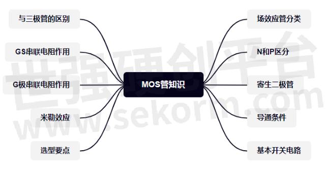
Fig.1
Field effect tube classification
There are two types of JFET and MOSFET.
The full English name of JFET -- Junction field-effect supply be visualized in either the N channel or P channel, which is virtually non-existent in reality.
The MOSFET is the metal-oxide -Semiconductor field-effect Transistor. It is widely used as a MOS Transistor.
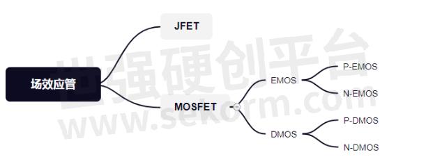
Fig.2
MOSFET can be divided into two categories: enhanced type and depleted type. Under each category are NMOS and PMOS.
The English word for the enhanced MOS tube is Enhancement MOS or EMOS, while the English word for the depleted MOS tube is Depletion MOS or DMOS.
The most commonly used motherboard is an enhanced MOS tube, NMOS is most commonly used in signal control, followed by PMOS, mostly used in power switches and other aspects, with almost no depletion type.
N and P
The following red arrow pointing to the G pole is NMOS, while the arrow pointing back to the G pole is PMOS.
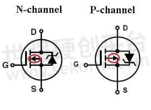
Fig.3
As can be seen from the figure above, the direction of NMOS and PMOS parasitic diodes is different. NMOS →D pole, while PMOS →S pole.
The parasitic diode is the same as the ordinary diode, the positive connection will lead and the reverse connection will cut off. For NMOS, when the S pole is connected to the positive, and the D pole to the negative, the parasitic diode will lead on, and vice versa. For the PMOS tube, when the D pole is connected to the positive, the S pole to the negative, parasitic diode conduction, and vice versa.
In some applications, stripper diodes are also selected to reduce the voltage drop between DS (the voltage drop of the bulk diodes is much larger than the on-off voltage drop of the MOS), as well as the over-current capability of the bulk diodes.
When meeting the MOS tube conduction condition, the D and S pole of MOS tube conduction, this time the body diode is by the state, because of the MOS tube conduction resistance tiny, general m Ω level, through the current of 1 a level, just also mV level, so the D and S pole conduction between the pressure drop is small, enough to reduce parasitic diode conduction, which needs special attention.
Conduction condition
MOS tube is a pressure-controlled type, and its conduction is determined by the pressure difference between G and S poles.
For NMOS, VG-VS >VGS(TH), i.e., the pressure difference between the G pole and the S pole is greater than a certain value, the MOS tube will conduct conduction, but it should not be too large, otherwise, the MOS tube will be burned out. The opening voltage and other parameters can be determined by the SPEC of the specific device.
For PMOS, VG-VS >VGS(TH), that is, the pressure difference between the S pole and the G pole is greater than a certain value, and the MOS tube will conduct. Similarly, the specific parameters depend on the SPEC of the device.
Basic switching circuit
NMOS switch circuit
When the GPIO_CTRL voltage is less than the MOS tube opening voltage, the MOS tube stops, and OUT is pulled up to 5V through R1, and OUT=5V.
When the GPIO_CTRL voltage is greater than the MOS tube opening voltage, the MOS tube is on, and the D-pole voltage is equal to the S-pole voltage, that is, OUT=0V.
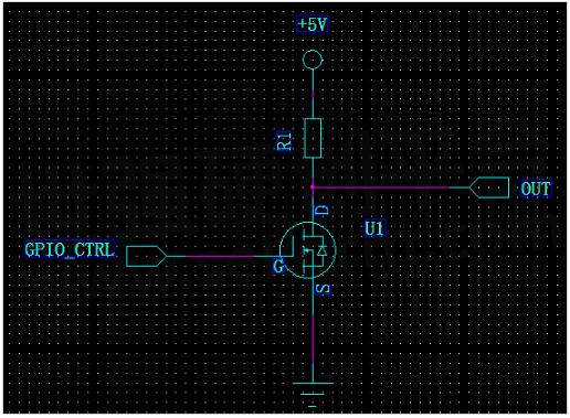
Fig.4
PMOS switch circuit
PMOS tube is most commonly used in power switching circuits. As shown in the following figure, when GPIO_CRTL=0V, the differential pressure between S and G is greater than the MOS tube opening voltage, MOS tube conducting, 5V_VOUT=5V_VIN.
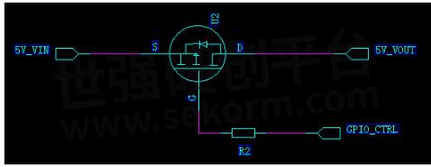
Fig.5
The difference with a triode
Triode is the current control, and MOS tube is the voltage control, there are mainly the following differences:
1. Choose an MOS tube when only a small amount of current is allowed from the signal source; Under the condition of low signal voltage and allowing more current to be taken from the signal source, a triode is selected.
2. The MOS tube is a unipolar device (conducting by a majority of carriers), and the audion is a bipolar device (conducting by both majority and minority carriers).
3. The source and drain of some MOS tubes can be used interchangeably, and the gate can be positive or negative, which is more flexible than the triode.
4. MOS tubes are widely used and can operate at very low current and voltage.
5, MOS tube input impedance is large, low noise, MOS tube is more expensive, the transistor loss is large.
6, MOS tube is commonly used as a power switch, as well as large current switching circuit, high frequency high-speed circuit, triode is commonly used for digital circuit switch control.
The effect of the series resistance of G and S poles
The MOS tube is a voltage-controlled type. In some cases, why do we need a resistor in series at the G pole?
1, slow down RDS from infinity to RDS(ON).
2. Avoid shock. Generally, the I/O output of the single chip microcomputer will have some stray inductance. In the case of voltage mutation, LC shock may be formed with the grid capacitance.
3. Reduce the peak current of gate charging.
Miller effect of MOS tube
About the Miller effect of MOS tube, you can read the article:http://www.HI-SEMICON.com/info-detail/id-27.html
Selection of the main points
1. The voltage value
Pay attention to the maximum VDS on-off voltage and the maximum VGS withstand voltage. In actual use, the value should not be exceeded, otherwise the MOS tube will be damaged.
Table.1

Pay attention to on voltage VGS(TH). Generally, MOS transistors are controlled by single-chip microcomputer. According to the level of GPIO of a single-chip microcomputer, MOS transistors with appropriate conduction threshold are selected, and a certain margin is left as far as possible to ensure that MOS can be switched normally.
Table.2
![]()
2. The current value
Pay attention to ID current. This value represents how much current can flow through the PMOS tube and reflects its ability to carry a load. Beyond this value, the MOS tube will also be damaged.
Table.3

3. Power loss
Power loss needs to be concerned with the following parameters, including thermal resistance and temperature. Thermal resistance refers to the ratio between the temperature difference at both ends of the object and the power of the heat source when heat is transmitted over the object. The unit of thermal resistance is ℃/W or K/W. The formula of thermal resistance is ThetaJA = (TJ-TA)/P, which is related to both power and ambient temperature.
Table.4

4. Conduction of internal resistance
Conduction resistance ON PMOS RDS (ON) parameters, the smaller the conduction resistance, the smaller the wastage of the PMOS tube, PMOS tube conduction resistance is in commonly m Ω level.
5. Switching time
MOS as a switching device, there will be the concept of switching time, in the high-speed circuit, as far as possible to choose the input and output capacitance CISS&COSS small, switch time Ton&Toff short MOS tube, to ensure normal data communication.
6. Packaging
According to the size of the PCB board, select the appropriate PMOS tube size, in the case of limited onboard area, choose the small package as far as possible; As far as possible select common packaging, to prepare for the subsequent selection of appropriate replacement material.
- |
- +1 赞 0
- 收藏
- 评论 0
本文由三年不鸣转载自HI-SEMICON News,原文标题为:MOS tube knowledge, must read!,本站所有转载文章系出于传递更多信息之目的,且明确注明来源,不希望被转载的媒体或个人可与我们联系,我们将立即进行删除处理。
相关推荐
【技术】MOSFET规格书参数详解
极限参数HI-SEMICON极限参数也叫绝对最大额定参数,MOS管在使用过程当中,任何情况下都不能超过下图的这些极限参数,否则MOS管有可能损坏。本文对MOSFET规格书参数进行详细讲解。
Miller Effect on MOS Tube Switches
The gate drive process of MOSFET can be simply understood as the charging and discharging process of the input capacitance (mainly CGS of the gate source capacitance) of the MOSFET. When THE CGS reaches the threshold voltage, MOSFET will enter the opening state.
Application of MOS and Rectifier in Blower Products
As a high-frequency electric product, hair dryer usually consists of heating wire, high-speed small fan and circuit board. There are usually metal blowers and plastic blowers, and the centrifugal airflow formed by the rotation of the blades driven by the motor drives the rotor to blow out to achieve the purpose of drying and shaping. In this issue, Heketai introduces the application of MOS and rectifier in hair dryer products.
KP1054XVP高集成度高效率降压LED电源开关
描述- KP1054XVP是一款高度集成的降压LED电源开关IC,适用于LED照明应用。该芯片集成500V功率MOSFET、600VFRD和功率控制器,并包含高压LDO供电电路和无VDD电容的单绕组电感变压器。
型号- KP1054XVP
MOS Tube HKTD20N06 with Continuous Drain Current of 20A, Can be Used in Motor Drive, LED and Power Supply Products
MOS transistor plays a very important role in voltage stabilizing and switching circuits. A good MOS transistor has not only good product performance, but also its power consumption and product stability. In this issue, Heketai introduces a MOS tube HKTD20N06, which can be used in motor drives, LEDs and power supplies.
MOS Switch Tube Selection and Principle Application
When the input voltage UI changes from high to low and the MOS tube changes from the on-off state to the cut-off state, the power UDD charges the stray capacitance CL via RD, charging time constant 1=RDCL, so the output voltage UO must pass a certain delay to change from the low level to the high level.
Switching Power Supply MOS Tube Loss
Switch Mode Power Supply, also known as switched Power Supply, switching converter, is a high-frequency Power conversion device, is a kind of Power Supply. Its function is to convert a potential voltage through different forms of architecture to the voltage or current required by the client. Switching power supplies convert voltages and currents between the inputs, which are mostly AC (such as mains power) or DC power, and the outputs, which are mostly devices requiring DC power, such as personal computers.
500V/20A N-channel Enhanced mode TO-220F/TO-247 MOSFET SW20N50D for Charger, Adaptor and LED
This power MOSFET SW20N50D is produced with advanced technology of SAMWIN. This technology enable the power MOSFET to have better characteristics, including fast switching time, low on resistance, low gate charge and especially excellent avalanche characteristics.
AS5P10ES P沟道增强型MOSFET
描述- 该资料详细介绍了AS5P10ES型号的P-Channel Enhancement Mode MOSFET(增强型MOSFET)的产品特性、电气特性、应用领域和封装信息。资料涵盖了该产品的最大额定值、静态和动态电气特性、典型特性以及SOP-8封装的尺寸信息。
型号- AS5P10ES
MOSFET的失效机理分析
当向MOSFET施加高于绝对最大额定值BVDSS的电压时,会造成击穿并引发雪崩击穿。发生雪崩击穿时,会流过大电流,存在MOSFET失效的危险。MOSFET雪崩失效包括短路造成的失效和热量造成的失效。本文介绍失效的机理原因。
Shindengen Announced the Launch of High Withstand Voltage 900V Power MOSFET based on AEC-Q101, Optimal for xEV High Voltage DC/DC Converters
Shindengen has launched two new products, the P3FH90VX3 and P5FH90VX3 power MOSFET based on the AEC-Q101 vehicle application reliability standards. The products‘ high withstand voltage of 900V prefers to install main switches and discharge circuit switches for xEV DC/DC converter control power supplies.
ZMS020N03NC 30V N沟道功率MOSFET
描述- ZMJ半导体公司推出的ZMS020N03NC是一款30V N-Channel Power MOSFET,采用先进的沟槽MOSFET技术和低电阻封装,提供极低的RDS(ON),适用于开关和电池保护应用。
型号- ZMS020N03NC
MOS Tube H Bridge Motor Drive Circuit Diagram
H bridge is a typical DC motor control circuit, because its circuit shape resembles the letter H, so it is named “H bridge“. Four audions constitute the four vertical legs of H, and the motor is the horizontal bar in H (note: the figure is only a schematic diagram, rather than a complete circuit diagram, in which the driving circuit of the audion is not drawn).
MOS tube structure principle
Structure and symbol (take n-channel enhanced type as an example) -- Two high-concentration N-type areas are diffused on a low-concentration P-type silicon as drain and source, the semiconductor surface is covered with a silicon dioxide insulation layer and an electrode is drawn as a gate.
G7P03S P沟道 MOSFET
描述- 该资料详细介绍了GOFORD公司生产的G7P03S P-Channel Trench MOSFET。该器件采用先进的沟槽技术,具有优异的RDS(ON)和低栅极电荷,适用于多种应用场景。资料中包含了产品特性、电气参数、应用领域和封装信息。
型号- G7P03S
电子商城
现货市场
服务
定制液冷板尺寸5mm*5mm~3m*1.8m,厚度2mm-100mm,单相液冷板散热能力最高300W/cm²。
最小起订量: 1片 提交需求>


登录 | 立即注册
提交评论