Explain in Detail the Cause of MOS Tube Heating


For power supply design or driving circuits, it is inevitable to use a field effect tube, which is often called an MOS tube. There are many kinds of MOS tubes and they have many functions. To do the use of power or drive, of course, is to use its switching action.
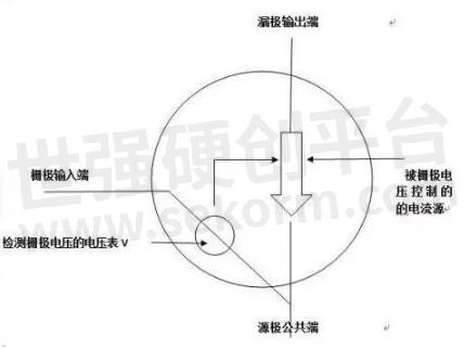
Regardless of N type MOS tube or P type MOS tube, the operating principle is essentially the same. MOS transistors control the drain current at the output end by applying a voltage to the gate at the input end. MOS tube is a voltage control device. It controls the characteristics of the device by adding voltage to the grid, which will not cause the charge storage effect caused by the base current when the triode is switched. Therefore, in switching applications, the switching speed of the MOS tube should be faster than that of the triode. Its main principles are as follows:

Fig.1
How the MOS tube works
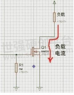
The open-drain circuit of the MOS tube is commonly used in switching the power supply. As shown in FIG. 2, the open-drain is connected to the load intact, which is called an open-drain circuit. No matter how high the load voltage is connected to the open-drain circuit, the load current can be switched on and off. It is an ideal analog switching device. This is the principle of MOS transistors as switching devices. Of course, there are many circuit forms used for MOS tube switches.

Fig.2 Open drain circuit of NMOS tube
In switching power applications, such applications require MOS tubes to be regularly switched on and off. For example, the basic step-down converters commonly used in DC-DC power supplies rely on two MOS transistors to perform the switching function. These switches alternately store energy in the inductor and release it to the load. We often choose frequencies of hundreds of kHz or even more than 1 MHz, because the higher the frequency, magnetic elements can be smaller and lighter. During normal operation, the MOS tube is only equivalent to a conductor. Therefore, what we circuit or power supply designers are most concerned with is the minimum conduction loss of MOS.
MOS tube manufacturers use RDS(ON) parameters to define the on-off impedance. For switching applications, RDS(ON) is also the most important device feature. The data sheet defines RDS(ON) as relating to the gate (or drive) voltage VGS and the current flowing through the switch, but for a full gate drive, RDS(ON) is a relatively static parameter. MOS tubes that are always on are easily heated. In addition, a slowly rising junction temperature will also lead to an increase in RDS(ON). The MOS tube data sheet specifies the thermal impedance parameters, which are defined as the semiconductor junction heat dissipation capability of the MOS tube package. The simplest definition of RθJC is the thermal impedance to the shell.
1. In the heating situation, the circuit design problem is to make the MOS tube work in the linear working state, rather than in the switching state. This is also a cause of MOS tube heating. If N-MOS is used as a switch, the G voltage must be several V higher than the power supply to fully conduct, while p-MOS is the opposite. The power consumption is caused by the high-pressure drop due to the incomplete opening. The equivalent DC impedance is relatively large, and the pressure drop increases. Therefore, U*I also increases, and the loss means the heating. This is the most taboo mistake in designing a circuit.
2. The frequency is too high, mainly because the excessive pursuit of volume sometimes leads to the increase of frequency, and the loss on the MOS tube increases, so the heating also increases
3. Insufficient heat dissipation design, too high current, MOS tube nominal current value, generally need good heat dissipation to achieve. Therefore, ID is less than the maximum current, and the heat may be severe, so sufficient auxiliary heat sinks are needed.
4. Wrong selection of MOS tube, wrong judgment on power, insufficient consideration of internal resistance of MOS tube, resulting in increased switching impedance.
- |
- +1 赞 0
- 收藏
- 评论 0
本文由三年不鸣转载自HI-SEMICON News,原文标题为:Explain in detail the cause of MOS tube heating,本站所有转载文章系出于传递更多信息之目的,且明确注明来源,不希望被转载的媒体或个人可与我们联系,我们将立即进行删除处理。
相关推荐
【经验】几种MOS管防反接防过压电路解析
关于MOS管防反接防过压电路您有了解吗?本文HI-SEMICON将为您介绍几种MOS管防反接防过压电路。当电源正确接入时。电流的流向是从V到负载,在通过NMOS到GND。刚上电时因为NMOS管的体二极管存在,地回路通过体二极管接通。
MOS Switch Tube Selection and Principle Application
When the input voltage UI changes from high to low and the MOS tube changes from the on-off state to the cut-off state, the power UDD charges the stray capacitance CL via RD, charging time constant 1=RDCL, so the output voltage UO must pass a certain delay to change from the low level to the high level.
MOS Tube Anti-overvoltage Circuit
When the power is properly connected. The current flows from VIN to the load, through NMOS to GND. At the beginning of power on, because the body diode of the NMOS tube exists, the ground circuit is connected through the body diode. Later, because the VGS is greater than the threshold voltage of VGSTH, the MOS tube conducts.
【经验】防反接电路、电平转换电路、锁相电路中的MOS管电路分析
只要我们了解MOS管的特征参数,遇到MOS管电路,再也不会被电路分析难倒了。对于MOS管电路功能,HI-SEMICON还有一些小技巧分享给大家,比如针对防反接电路、逻辑电平转换电路、锁相电路,大家在用的时候可以手到擒来!
Details of MOS tube packaging
After the MOS tube chip is made, a shell is needed to be added to the MOS tube chip, which is the MOS tube package. The package housing mainly plays the role of support, protection and cooling, and also provides electrical connection and isolation for the chip, so as to form a complete circuit between MOS tube devices and other components. Different packaging, different design, MOS tube specifications, size, various electrical parameters, etc. will be different, and they can play a different role in the circuit will be different.
MOS Tube and Simple CMOS Logic Level Circuit
Take n-type tube as an example, and the 2 ends are the control ends, which are called “gate“. The 3-terminal is usually grounded and is referred to as the “source“; The source voltage is denoted as VSS, the positive voltage at the end is called “drain“, and the drain voltage is denoted as VDD. To enable terminal 1 and terminal 3 to conduct, the level on gate 2 must be increased.
Switching Power Supply MOS Tube Loss
Switch Mode Power Supply, also known as switched Power Supply, switching converter, is a high-frequency Power conversion device, is a kind of Power Supply. Its function is to convert a potential voltage through different forms of architecture to the voltage or current required by the client. Switching power supplies convert voltages and currents between the inputs, which are mostly AC (such as mains power) or DC power, and the outputs, which are mostly devices requiring DC power, such as personal computers.
Miller Effect on MOS Tube Switches
The gate drive process of MOSFET can be simply understood as the charging and discharging process of the input capacitance (mainly CGS of the gate source capacitance) of the MOSFET. When THE CGS reaches the threshold voltage, MOSFET will enter the opening state.
Is It Always Difficult to Use and Replace MOS Tubes for Multimeter Tests?
MOS tube has always been one of the topics that engineers are keen to discuss, so we have sorted out the common and uncommon knowledge of MOS tube, hoping to be of some help to engineers. Now let‘s talk about the MOS tube, a very important component. Antistatic protectionAlthough the MOS tube has internal protection measures, we should also operate by the anti-static operation rules, which qualified maintenance personnel should have.
MOS Tube Knowledge, Must Read!
According to the size of PCB board, select the appropriate PMOS tube size, in the case of limited on-board area, choose the small package as far as possible; As far as possible to select common packaging, to prepare for the subsequent selection of appropriate replacement material.
MOS tube structure principle
Structure and symbol (take n-channel enhanced type as an example) -- Two high-concentration N-type areas are diffused on a low-concentration P-type silicon as drain and source, the semiconductor surface is covered with a silicon dioxide insulation layer and an electrode is drawn as a gate.
MOS Tube Drive Circuit Summary - Detailed Design of Various Switching Power Supply MOS Tube Drive Circuit
When using MOS tube drive circuit to design switch power supply or motor drive circuit, most people will consider MOS conduction resistance, maximum voltage, maximum current, etc., and many people only consider these factors. Such circuits may work, but they are not excellent and are not allowed as a formal product design.
MOS Tube H Bridge Motor Drive Circuit Diagram
H bridge is a typical DC motor control circuit, because its circuit shape resembles the letter H, so it is named “H bridge“. Four audions constitute the four vertical legs of H, and the motor is the horizontal bar in H (note: the figure is only a schematic diagram, rather than a complete circuit diagram, in which the driving circuit of the audion is not drawn).
Experience sharing of classical MOS transistor level conversion circuit
Level switch in the circuit design is very common, because of circuit design, most of the time just like in the building blocks of the circuit module, and the circuit module, patchwork together is a electronic products. However, the voltage domain is often inconsistent between modules, so the level conversion circuit is used for the communication between modules.
To Prevent MOS Tube from Burning, We Need to Know Why it Burns First
MOS working state in the controller circuit: on process (transition process from conduction to cut-off), on state, off process (transition process from conduction to cut-off), and cut-off state.The MOS major losses also correspond to the following states: switch losses (on and off), conduction losses, cut-off losses (caused by leakage current, which is ignored), and avalanche energy losses.
电子商城
现货市场
服务
定制液冷板尺寸5mm*5mm~3m*1.8m,厚度2mm-100mm,单相液冷板散热能力最高300W/cm²。
最小起订量: 1片 提交需求>
可定制位移传感器量程范围10~600mm,该YWD型位移传感器表面有带刻度的透明窗☐,每毫米的变化量误差不超过3ue/mm,可在静态、准静态和低频动态下工作。主要指标:非线性<0.2%;供桥电压<10v;测试精度:0.01mm。
最小起订量: 1 提交需求>


登录 | 立即注册
提交评论