MOS Tube and Simple CMOS Logic Level Circuit


MOS tubes are of two types: N-type and P-type
As shown in the figure below:
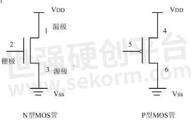
Fig.1
Take n-type tube as an example, and the 2 ends are the control ends, which are called "gate". The 3-terminal is usually grounded and is referred to as the "source"; The source voltage is denoted as VSS, the positive voltage at the end is called "drain", and the drain voltage is denoted as VDD. To enable terminal 1 and terminal 3 to conduct, the level on gate 2 must be increased.
For p-type tube, gate, source and drain terminals are 5 end, 4 end and 6 end respectively. To enable 4-end and 6-end conduction, gate 5 should be added to the low level.
In the logic devices made by CMOS technology or single chip microcomputer, N-type tube and P-type tube often appear in pairs. The two CMOS tubes that appear at the same time are called "complementary CMOS tubes" as long as one is on and the other is not on (i.e., "cut off" or "off") at any time.
2. CMOS logic level
The power supply voltage VDD of high-speed CMOS circuit is usually +5V. VSS grounding, it's 0V.
High level is regarded as logic "1", and the level value ranges from 65% to VDD(or VDD-1.5V to VDD).
Low levels are considered logic "0" and are required to be no more than 35% of VDD or 0 ~ 1.5V.
+1.5V ~ +3.5V should be considered as uncertain level. Uncertain levels should be avoided in hardware design.
In recent years, with the development of sub-micron technology, the power supply of single-chip microcomputer is decreasing. Low power voltage helps to reduce power consumption. CMOS devices with VDD of 3.3V have been widely used. In portable applications, VDD is 2.7V, and even 1.8V microcontroller has appeared. In the future, the supply voltage will continue to decline to 0.9V, but a level lower than 35% of VDD will be regarded as logic "0", while a level higher than 65% of VDD will be regarded as logic "1".
3.Gate
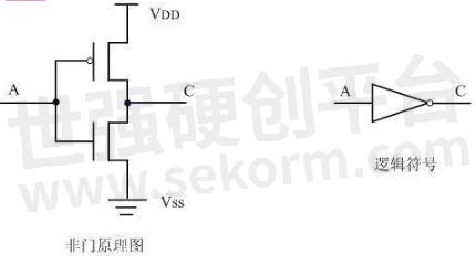
Fig.2
Non - gate (inverters) is the simplest gate circuit, consisting of a pair of CMOS tubes. Its working principle is as follows:
A terminal is at high level. The P-type tube is off and the N-type tube is on. The level of the output terminal C is consistent with Vss and the output is low. The A end is at low level, the P-type tube is on and the N-type tube is off. The level of the output end C is consistent with that of VDD, and the output level is high.
4. The nand gate
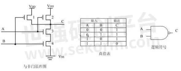
Fig.3
And non gate working principle:
A, B input are all low power, 1, 2 tube conduction, 3, 4 tube cutoff, C terminal voltage and VDD consistent, output high level.
A input high level, B input low level at ordinary times, 1, 3 tube conduction, 2, 4 tube cutoff, C end potential and 1 tube drain to maintain the same, output high level.
A input low level, B input high level normally, the situation is similar to, also output high level.
A, B input are high power, 1, 2 tube cutoff, 3, 4 tube conduction, C terminal voltage and ground consistent, output low level.
5. Nor gate
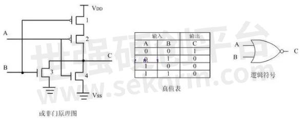
Fig.4
Or non-gate working principle:
A, B input are all low power, 1, 2 tube conduction, 3, 4 tube cutoff, C terminal voltage and VDD consistent, output high level.
A input high level, B input low level, 1, 4 tube conduction, 2, 3 tube cutoff, C-end output low level.
A input low level, B input high level, the situation is similar to, also output low level.
A, B input are high power, 1, 2 tube cutoff, 3, 4 tube conduction, C terminal voltage and ground consistent, output low level.
Note:Remove the small circle at the output end of the above "and neither" gate and "or" gate logic symbol to become the logical symbol of "and" gate and "or" gate. The circuit diagram of realizing the function of "and", "or" must add a inverter at the output end, that is, add a pair of CMOS tubes, therefore, "and" gate is actually more complex than "and not" gate, the delay time is also longer, this point should be paid attention to in the circuit design.
6. Three states

Fig.5
Working principle of tri-State gate:
When the control end C is "1", the n-type tube 3 conducts. At the same time, the level of C-end becomes low after passing through the reverter, so that the P-type tube 4 conducts, and the level of input end A can reach the output end B through 3 or 4 tubes.
When the control end C is "0", the 3 and 4 tubes are all cut off, and the level of input end A cannot reach the output end B. The output end B presents A state of high resistance, which is called "high resistance state".
This device is also known as a "transport gate with a control end". Tri-state gates with a certain drive capability are also called "buffers" and have the same logical notation.
Note:It can be seen from the CMOS equivalent circuit, truth table and logical expression that by changing the position of "0" and "1", the "and not" gate becomes the "or not" gate. The signal that is valid for "1" is the "and not" relation, and the signal that is valid for "0" is the "or not" relation.
The symbols of logic devices in the above figure are the input and output relations under positive logic, that is, they are valid for "1" (high level). However, most of the control signals in MCU are defined in terms of negative validity (low level validity). For example, Chip Select signal CS(Chip Select) refers to the meaning marked by characters when the signal is "0", that is, the signal is "0", indicating that the Chip is selected. Therefore, the logical symbol of the "or not" gate can also be drawn as below.
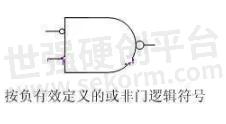
Fig.6
7. Combinational logic circuit
Various combinational logic circuits, such as decoder, decoder and multiplexer, can be obtained from different combinations of logic circuits, such as "and non" gate, "or non" gate, etc.
Combinational logic circuits can be implemented using off-the-shelf integrated circuits or programmable logic devices such as PAL, GAL, and so on.
- |
- +1 赞 0
- 收藏
- 评论 0
本文由三年不鸣转载自HI-SEMICON News,原文标题为:MOS tube and simple CMOS logic level circuit,本站所有转载文章系出于传递更多信息之目的,且明确注明来源,不希望被转载的媒体或个人可与我们联系,我们将立即进行删除处理。
相关推荐
MOS Switch Tube Selection and Principle Application
When the input voltage UI changes from high to low and the MOS tube changes from the on-off state to the cut-off state, the power UDD charges the stray capacitance CL via RD, charging time constant 1=RDCL, so the output voltage UO must pass a certain delay to change from the low level to the high level.
MOS Tube Anti-overvoltage Circuit
When the power is properly connected. The current flows from VIN to the load, through NMOS to GND. At the beginning of power on, because the body diode of the NMOS tube exists, the ground circuit is connected through the body diode. Later, because the VGS is greater than the threshold voltage of VGSTH, the MOS tube conducts.
Switching Power Supply MOS Tube Loss
Switch Mode Power Supply, also known as switched Power Supply, switching converter, is a high-frequency Power conversion device, is a kind of Power Supply. Its function is to convert a potential voltage through different forms of architecture to the voltage or current required by the client. Switching power supplies convert voltages and currents between the inputs, which are mostly AC (such as mains power) or DC power, and the outputs, which are mostly devices requiring DC power, such as personal computers.
Miller Effect on MOS Tube Switches
The gate drive process of MOSFET can be simply understood as the charging and discharging process of the input capacitance (mainly CGS of the gate source capacitance) of the MOSFET. When THE CGS reaches the threshold voltage, MOSFET will enter the opening state.
MOS Tube Knowledge, Must Read!
According to the size of PCB board, select the appropriate PMOS tube size, in the case of limited on-board area, choose the small package as far as possible; As far as possible to select common packaging, to prepare for the subsequent selection of appropriate replacement material.
Is It Always Difficult to Use and Replace MOS Tubes for Multimeter Tests?
MOS tube has always been one of the topics that engineers are keen to discuss, so we have sorted out the common and uncommon knowledge of MOS tube, hoping to be of some help to engineers. Now let‘s talk about the MOS tube, a very important component. Antistatic protectionAlthough the MOS tube has internal protection measures, we should also operate by the anti-static operation rules, which qualified maintenance personnel should have.
MOS Tube H Bridge Motor Drive Circuit Diagram
H bridge is a typical DC motor control circuit, because its circuit shape resembles the letter H, so it is named “H bridge“. Four audions constitute the four vertical legs of H, and the motor is the horizontal bar in H (note: the figure is only a schematic diagram, rather than a complete circuit diagram, in which the driving circuit of the audion is not drawn).
MOS tube structure principle
Structure and symbol (take n-channel enhanced type as an example) -- Two high-concentration N-type areas are diffused on a low-concentration P-type silicon as drain and source, the semiconductor surface is covered with a silicon dioxide insulation layer and an electrode is drawn as a gate.
Explain in Detail the Cause of MOS Tube Heating
For power supply design or driving circuit, it is inevitable to use field effect tube, which is often called MOS tube. There are many kinds of MOS tubes and they have many functions. To do the use of power or drive, of course, is to use its switching action.Regardless of N type or P type MOS tube, the operating principle is essentially the same. MOS transistors control the drain current at the output end by applying voltage to the gate at the input end. MOS tube is a voltage control device.
Details of MOS tube packaging
After the MOS tube chip is made, a shell is needed to be added to the MOS tube chip, which is the MOS tube package. The package housing mainly plays the role of support, protection and cooling, and also provides electrical connection and isolation for the chip, so as to form a complete circuit between MOS tube devices and other components. Different packaging, different design, MOS tube specifications, size, various electrical parameters, etc. will be different, and they can play a different role in the circuit will be different.
Hardware Necessary Skills, MOS Tube Composed of Basic Gate Logic Circuit
As a hardware engineer, you can‘t help but understand chips. In order to understand the chip, the basic logic circuits composed of MOS tubes must be memorized so as to be able to understand the chip block diagram more proficiently. The field-effect Transistor provides a variety of gate circuits that can be visualized in a variety of combinations or visuals that, as the description in the beginning, may be the basis of a modern IC.
MOS Tube Drive Circuit Summary - Detailed Design of Various Switching Power Supply MOS Tube Drive Circuit
When using MOS tube drive circuit to design switch power supply or motor drive circuit, most people will consider MOS conduction resistance, maximum voltage, maximum current, etc., and many people only consider these factors. Such circuits may work, but they are not excellent and are not allowed as a formal product design.
Experience sharing of classical MOS transistor level conversion circuit
Level switch in the circuit design is very common, because of circuit design, most of the time just like in the building blocks of the circuit module, and the circuit module, patchwork together is a electronic products. However, the voltage domain is often inconsistent between modules, so the level conversion circuit is used for the communication between modules.
Why are MOS tubes broken down by static electricity,and what should we do about it?
MOS tube a ESD sensitive devices, its input resistance is very high, and the gate electrode capacitance is very small, so vulnerable to external electromagnetic or electrostatic induction and charged (a small amount of charge on the interelectrode capacitance can form a very high voltage (think U = Q/C) will be pipe damage, and because of the strong electrostatic situation difficult to charge and discharge to electrostatic breakdown.
To Prevent MOS Tube from Burning, We Need to Know Why it Burns First
MOS working state in the controller circuit: on process (transition process from conduction to cut-off), on state, off process (transition process from conduction to cut-off), and cut-off state.The MOS major losses also correspond to the following states: switch losses (on and off), conduction losses, cut-off losses (caused by leakage current, which is ignored), and avalanche energy losses.
电子商城
服务
定制液冷板尺寸5mm*5mm~3m*1.8m,厚度2mm-100mm,单相液冷板散热能力最高300W/cm²。
最小起订量: 1片 提交需求>
可烧录IC封装SOP/MSOP/SSOP/TSOP/TSSOP/PLCC/QFP/QFN/MLP/MLF/BGA/CSP/SOT/DFN;IC包装Tray/Tube/Tape;IC厂商不限,交期1-3天。支持IC测试(FT/SLT),管装、托盘装、卷带装包装转换,IC打印标记加工。
最小起订量: 1pcs 提交需求>


登录 | 立即注册
提交评论