What is a Chiplet, and Why Should You Care?

Chiplets are a new way to build system-on-chips (SoCs) that can improve yields and reduce costs by more than 45%. It partitions the chip into discrete elements and connects them with a standardized interface, allowing designers to meet performance, efficiency, power, size, and cost challenges in the 5/6G, AI, and VR era.
Unlike monolithic SoCs, chiplets enable an open ecosystem of modular components that can be reused and customized. But what exactly is a chiplet and what are the advantages of using it?
What is a Chiplet?
A chiplet is a small, modular chip that performs a specific function very well. For example, a chiplet can be a processor core, a memory block, an I/O driver, or a signal processing unit. Chiplets are designed to be used in a chiplet-based architecture, in which multiple chiplets are connected through a standardized high-speed digital interface to form a complete system-on-chip (SoC).
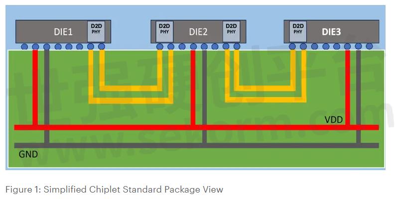
This way, you can create complex and powerful SoCs by mixing and matching different functions and technologies to create a customized system without having to fit all the components onto a single monolithic chip.
What are the Benefits of Chiplets?
There are several key benefits of adopting chiplet technology:
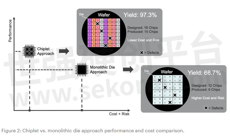
· Optimized Performance and Power: Chiplets can be optimized for their specific functions and technologies, improving the SoC's performance and power efficiency. Chiplets can also be placed closer together, reducing the interconnects' latency and power consumption.
· Lower Manufacturing Cost: Chiplets can be fabricated using different process nodes and foundries, which reduces the cost and risk of producing large, complex chips. Chiplets can also be reused across different SoCs, which increases the return on investment and reduces the time-to-market.
· Higher Flexibility and Scalability: Chiplets can be easily added or removed to adjust the functionality and performance of the SoC. Chiplets can also be updated or replaced without affecting the rest of the SoC, which enables faster innovation and adaptation to changing market demands.
How are Chiplets Changing the SoC Design?
Chiplets are revolutionizing the SoC design by enabling a new level of heterogeneity and modularity. Chiplets allow designers to leverage the best of different technologies and domains, such as logic, memory, analog, RF, and photonics, to create high-performance and power-efficient electronics.
It enables a new paradigm of design automation, in which chiplets can be selected, assembled, and optimized to create highly customizable SoC that meets specific design objectives and constraints.
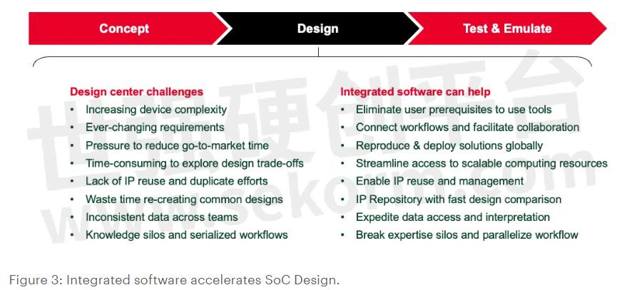
As a result, the design workflow is becoming highly iterative, and the traditional design center’s approach, which is very serialized, is becoming very time-consuming and inefficient.
Designers will need agility and cross-function collaboration to meet technology and market demands. This includes better concept, design, and simulation tools that reduce time-to-insight, eliminate unnecessary prototype spins, and remove knowledge silos.
And that’s where KEYSIGHT’s Modern Design Center approach comes in. It uses tightly integrated software to enable reproducible and scalable automation, allowing designers to focus on where it matters the most: assessing and validating electronic designs more confidently and collaboratively.
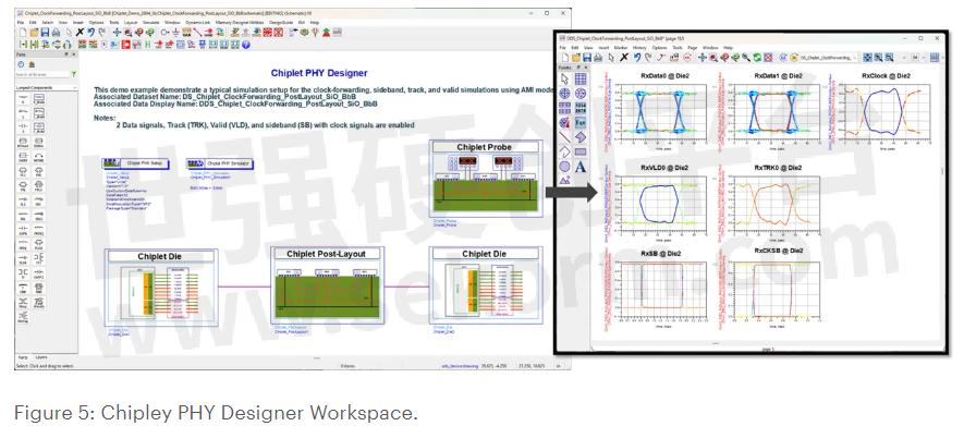
For example, Keysight EDA Chiplet PHY Designer, part of the Keysight EDA Advanced Design System (ADS), provides designers with a higher-level abstraction layer to explore a broader range of design scenarios simulating UCIe, measuring VTF, and analyzing forward clocking without spending time with manual and repetitive tasks.
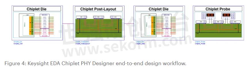
Keysight EDA Chiplet PHY Designer helps chiplet designers model and analyze chiplets from D2D PHY to D2D PHY at a system level (D2D: Die to Die PHY) using an intelligent design environment.
It includes a PHY designer and simulator, a via designer, a controlled impedance line designer (CILD), and an EM designer that enables the creation and import of parameterized 3D components into Keysight EDA ADS.
Simply put, Keysight EDA Software enables designers to create more complex and sophisticated designs in less time collaboratively.
Conclusion
Chiplets are a promising alternative to monolithic SoCs that offer lower costs, higher performance, and greater flexibility. Chiplets are also a key enabler of heterogeneous and modular SoC design, which can accelerate innovation and adaptation in the electronic industry. Keysight Modern Design Center enables reproducible and scalable automation so designers can pathfind for next-generation technologies more confidently.
- |
- +1 赞 0
- 收藏
- 评论 0
本文由雪飘梦飞转载自Keysight Blogs,原文标题为:What is a Chiplet, and Why Should You Care?,本站所有转载文章系出于传递更多信息之目的,且明确注明来源,不希望被转载的媒体或个人可与我们联系,我们将立即进行删除处理。
相关研发服务和供应服务
相关推荐
如何在ADS中进行通道仿真?
在评估高速通道的性能时,过去经常采用瞬态仿真(Transient simulation)来查看接收端的时域特性,但是随着信号速率的不断增加,我们需要考虑的因素越来越多,或者说之前不起眼的因素会对我们的信号质量产生严重的影响。为了解决上述问题,KEYSIGHT推出了通道仿真解决方案,这篇文章就来学习如何在ADS中进行通道仿真,以及通道方针所涉及的一些问题。

【经验】串扰问题产生的原因及解决办法、串扰仿真与测试
普通消费类电子产品的PCB电路板都至少都是四层,六层甚至以上。当两个不同的高速信号传播路径太靠近,他们彼此的电磁场就会互相影响,发生串扰。当然,串扰产生的实际原因要复杂得多,为了能更好的解决串扰问题,本文介绍了串扰产生机理、解决办法,还介绍了是德科技的PathWave ADS仿真软件仿真PCB串扰,结合是德科技的网络分析仪和PLTS软件进行串扰测试。

【经验】想要制作自定义的ADS设计套件吗?先来看看ADS原理图元件库的制作过程
ADS是工程师用于各种高频和高速电路与系统设计应用的主力工具,覆盖芯片,模块,板级设计,要使用该设计环境并利用其仿真功能,设计人员应具有链接到模型文件或仿真数据的元件库,设计套件即是以设计师为本的元件库工具包。本文介绍了自定义的ADS设计套件的过程。

介绍模拟电路的仿真软件应用
ADS软件应用领域广泛,涵盖通信系统设计、卫星通信、毫米波雷达、汽车雷达和射频集成电路设计等领域。在通信系统设计中,ADS软件可用于优化无线通信系统的前端电路,提高信号传输质量和系统的性能。在卫星通信中,ADS可帮助工程师设计和仿真卫星通信链路,提升传输效率和系统性能。在毫米波雷达和汽车雷达领域,ADS的仿真和分析功能有助于提高雷达系统的探测精度、抗干扰性和可靠性。

什么是X参数?X参数和S参数有什么区别?
本文以 ADS 软件电路仿真为例,由 Hot S22 引入了 X参数的概念;并介绍了 X 参数的实验设计,使用 ADS电路仿真,通过三次不同的仿真条件下得到的结果进行运算得到 X参数中的几个分量,并于 ADS软件直接提取的 X参数进行了对比。

是德科技解析ADS软件的功能和用途
为了设计高性能的电路并评估其性能,工程师需要使用先进的设计和仿真工具,ADS就是比较主流的一个软件。那么ADS是什么软件?ADS软件是干什么的?下面介绍一下ADS软件的功能和用途。

是德科技的PathWave ADS仿真软件,可以轻松仿真PCB串扰,加速产品开发流程
是德科技的PathWave ADS仿真软件,可以轻松仿真PCB串扰,结合是德科技的网络分析仪和PLTS软件进行串扰的测试,可以完成从概念设计、仿真、原型机设计、验证到生产制造和部署的全流程管理,从而加速产品开发流程。

【应用】Keysight ADS CILD和SIPro助力PCIE 5.0设计layout前后验证
本文主要介绍了PCIE 5.0主要指标、PCIE 5.0 设计面对的挑战、应对PCIE5.0设计挑战和PCIe 5.0仿真实例;突出了是德科技在开发中所提供的完美解决方案优势,针对于PCIE 5.0 设计面对的挑战,在Keysight ADS中,CILD和SIPro两个工具,可以分别满足PCIE 5.0 设计 layout前后的验证要求。

解析混动汽车和电动汽车DC/DC变换器的工作原理、设计和测试
本文是德科技首先介绍了混动汽车工作原理,并对混动汽车和电动汽车的直流对直流转换器进行设计和测试,给出了具体的设计模型及测试结果。

ADS与PCB协同仿真?是德科技的ADS软件成最主流的仿真工具
在进行射频PCB电路设计的时候,我们一般靠“经验”和“原则”指导设计,某些情况经验的作用也是有限的。要设计好射频板级电路,仿真是必不可少的。之所以某些经验可以替代仿真,是因为产品的电路非常成熟或集成化程度较高,对于创新型的设计,单纯依赖经验往往是不够的。科学的方法是将PCB封装和元器件仿真模型进行Co-Simulation半实物仿真,是德科技的ADS软件是最主流的仿真工具。

【经验】基于是德科技PathWave SystemVue的IBIS AMI建模方案详解
目前市场上能提供AMI模型建立以及测试工具的厂商很少,是德科技的PathWave SystemVue以及PathWave ADS(Advanced Design System)是目前市场上被广泛采用的工具。

接口总线标准的仿真设计与测试技术发展趋势
高速数字电路设计与测试技术发展近十多年来,数字集成电路和各种接口总线标准的发展令人眼花缭乱,目不暇接。各个总线标准通常由不同团队制订,其纷繁芜杂的测试和测量技术给从业人员带来许多困扰。本文将就当下的一些主要接口总线标准的仿真设计与测试技术发展趋势作一些简明的总结和说明。

【应用】Keysight ADS提供通用的PAM4 PRBS源和TX/RX模型助力光模块设计与仿真
Keysight ADS提供通用的PAM4 PRBS源和TX/RX模型助力光模块设计与仿真技术,本文介绍了高速光模块的电路设计与仿真。

如何在ADS中进行通道仿真
为了解决这些问题我们就必须采用一些均衡(EQ)措施,或者采用编码等方法。此外,由于处理的数据量增加,瞬态仿真非常的耗时间,这样看来瞬态仿真就显得力不从心了。为了解决上述问题,Keysight推出了通道仿真解决方案,学习如何在ADS中进行通道仿真,以及通道方针所涉及的一些问题。

是德科技电磁仿真软件RFPro成功验证支持Intel Foundry的Intel 18A工艺技术
是德科技宣布,RFPro电磁(EM)仿真软件作为是德科技EDA先进设计系统(ADS)综合工具套件中的一员,现已通过Intel Foundry认证,可帮助设计工程师开发采用Intel 18A工艺技术的设计。射频集成电路(RFIC)设计团队可结合使用这一全新的EM仿真功能和用于Intel 18A电路和物理设计的工艺设计套件(PDK),一次性设计出成功的产品。

电子商城


现货市场

服务
提供是德(Keysight),罗德(R&S)测试测量仪器租赁服务,包括网络分析仪、无线通讯综测仪、信号发生器、频谱分析仪、信号分析仪、电源等仪器租赁服务;租赁费用按月计算,租赁价格按仪器配置而定。
提交需求>
朗能泛亚提供是德(Keysight),罗德(R&S)等品牌的测试测量仪器维修服务,包括网络分析仪、无线通讯综测仪、信号发生器、频谱分析仪、信号分析仪、电源等仪器维修,支持一台仪器即可维修。
提交需求>
授权代理品牌:集成电路


授权代理品牌:分立元件


授权代理品牌:接插件及结构件


授权代理品牌:部件、组件及配件


授权代理品牌:电源及模块


授权代理品牌:电子材料


授权代理品牌:仪器仪表及测试配组件


授权代理品牌:电工工具及材料


授权代理品牌:机械电子元件


授权代理品牌:加工与定制


登录 | 立即注册
提交评论