An Introduction to Semiconductor Device Modeling


In the semiconductor IC design field, packing over 1 trillion transistors in a single processor is becoming the standard. With the process technology advancing toward 2 nanometer (nm) process nodes and lower, smaller device sizes introduce additional unforeseen effects at the nanoscale, uncharted in older technologies.
Accurately modeling such semiconductor devices is becoming increasingly complex each year. Engineers must determine hundreds of parameters to accurately predict the behavior of these devices across various sizes and temperatures. To deliver high-quality semiconductor designs faster, engineers need powerful device modeling tools.
In this article, you’ll learn about modern device modeling and its challenges. You’ll gain an understanding of device modeling flow, the role of device modeling in the design process, what goes into a device model, and which device models and modeling tools are available.
What Is Device Modeling?
Device modeling is the creation of mathematical models and formulas that describe the characteristics and behaviors of semiconductor devices, under different operating conditions.
The characteristics include:
· Electrical properties like voltages, currents, and capacitances under direct current (DC) and alternating current (AC) signals
· Electromagnetic (EM) and radio frequency (RF) characteristics like S-parameters and noise
The behaviors include phenomena like semi-conduction, thermal, and quantum effects.
Why Is Semiconductor Device Modeling Important?
Semiconductor devices are getting increasingly complex. Complex ICs like systems-on-a-chip (SoCs) and extreme miniaturization like the three-nanometer process are becoming common. These introduce a variety of complications like noise and heating.
To cope with such complex requirements, engineers use device modeling software to thoroughly understand, predict, and optimize the behaviors of devices.
This provides the following enormous benefits to device makers:
· Satisfies complex requirements: Device modeling helps engineers simulate different operating conditions and optimize their designs.
· Reduces costs: Each spin cycle (i.e., a round of design and fabrication) incurs higher fabrication costs. Virtual iterations are far cheaper.
· Shortens the time to market: Spin cycles also mean a longer time to market. Device modeling enables fast iterations with incremental improvements.
· Increases reliability: Device modeling confers long-term reliability, which means satisfied customers.
Which Semiconductor Devices Are Modeled?
Some of the common semiconductor devices that are analyzed using device modeling tools include:
· Various field effect transistors (FETs) like metal-oxide-semiconductor FETs (MOSFETs), junction FETs, and FinFETs
· High electron mobility transistors (HEMTs) like gallium nitride HEMTs (GaN HEMTs)
· Bipolar junction transistors
· Complementary metal oxide semiconductor (CMOS) devices
· Very large-scale integration (VLSI) devices like amplifier ICs and SoCs
· Transferred electron devices
· Diodes
· Integrated passive elements
Who Publishes Device Models, and Who Uses Device Models?
Companies that design such semiconductor devices use device modeling techniques extensively and provide their device models to customers. Many design companies are fabless — they don't do the physical fabrication themselves but outsource to foundries like TSMC. Others are integrated device manufacturers (IDMs) that design as well as fabricate.
At a higher level, system integrators are companies that target particular applications and industries by building circuits and equipment consisting of semiconductor devices. They use the device models from device companies in circuit simulation software like SPICE (Simulation Program with Integration Circuit Emphasis).
The Role of Device Modeling in Device Design
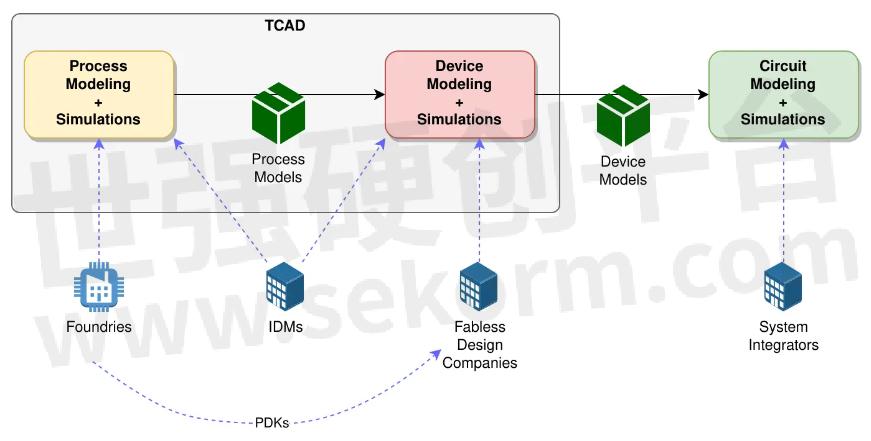
In this section, we'll first give a high-level overview of where device modeling fits in the overall design process when using electronic design automation (EDA) and its subfield, technology computer-aided design (TCAD). We go into more detail in later sections.
Process Modeling and Simulation
In the process modeling phase, the fabrication processes for the planned device are simulated and optimized virtually using TCAD software like process simulators.
These tools enable virtual fabrication. They can simulate steps like doping, etching, deposition, and oxidation, which alter the structural and chemical properties of the material layers. Process modeling predicts the resulting impurity profiles, layer thicknesses, and wafer topographies after each process step.
In the case of fabless designers, fabrication foundries do most of the process modeling and provide their manufacturing process models as process development kits (PDKs) to help designers meet device performance, power, and area targets quickly.
However, IDMs often do the process modeling themselves since they fabricate in-house, especially when using proprietary techniques based on their intellectual property.
Device Modeling and Device Simulation
In the device modeling phase, the goal is the mathematical characterization of the physical, electrical, thermal, and other behaviors of the device.
Device designers do most of the modeling and simulations and produce the device models for their customers. Some of the models and parameters from the previous process modeling are used in this phase.
Circuit Modeling and Simulation
In this phase, circuit designers in system integrator companies seek to understand how their circuit behaves under different operating conditions. Some of the device models that are optimized for simulation are used with circuit simulation software like Advanced Design System (ADS).
Types of Device Models
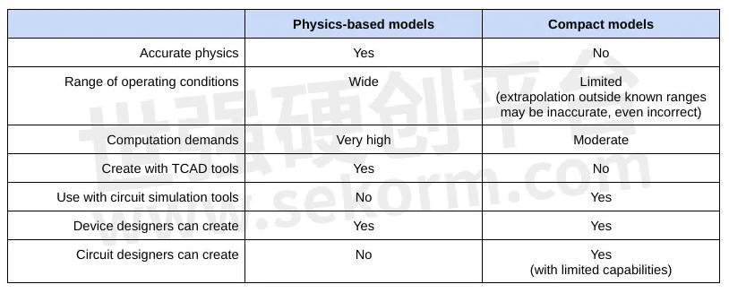
The device modeling phase can produce three types of models:
· Physics-based models: They're useful for exploring new device architectures or new materials by simulating semiconductor, quantum, thermal, EM, and RF phenomena.
· Compact models: They're used in high-level electrical simulations of integrated circuits and circuit boards. Some are derived from or simplified versions of physics-based models. Others are empirically determined from experimental data.
· Artificial neural network (ANN) models: For complex devices like thin-film transistors, memristors, or photonics semiconductors, compact models may take weeks or months to become available and may not have the desired level of accuracy at first. You can alleviate those problems by quickly training empirical, nonlinear ANN models instead of using a fully automated pattern extraction process. Such ANN models predict desired output parameters (like drain voltages) by learning the hidden patterns in high-dimensional, high-volume data consisting of dozens or even hundreds of measured parameters, like I-V, S-parameters, gate voltages, drain voltages, temperatures, and so on.
In general, physics-based models have better scalability for various operating conditions. Other differences are depicted below:
Physics-Based Device Modeling
In the design modeling and simulation phase, device designers focus on the physics-based modeling of:
· Properties of semiconductor materials (silicon or III-V compounds), like bandgap, electron mobility, Fermi levels, and dielectric constants
· Carrier generation and recombination
· Transport mechanisms like drift, diffusion, and tunneling
· Effects of layer dimensions and geometries
· Boundary conditions at substrate and other interfaces
· Nanoscale quantum mechanical effects
· Thermal behavior
· Polarization behaviors of direct bandgap semiconductors used in optoelectronics
· Effects of manufacturing parameters from the previous process modeling phase
TCAD vendors implement these mathematical models in their software with the necessary front-end and backend support. Device designers incrementally refine their models by iterating these steps:
· Device designers enter all the specifics and dimensions of their proposed designs.
· The TCAD software simulates the phenomena over time or under various environmental conditions using techniques like finite element methods.
· The calculated model parameters, results, and graphs are analyzed against experimental or ideal data.
· Any design issues or optimization bottlenecks are addressed by tweaking the proposed design, and the steps above are repeated.
Compact Device Modeling
Compact device modeling produces simplified empirical models that are useful for understanding the electrical behaviors of the device and can be used directly in electrical circuit simulations.
They may be simplified versions of physics-based models and also incorporate parameters from the process models.
Compact models typically contain a core set of models and formulas for predicting, under various operating conditions, the device's electrical properties like:
· Current-voltage (I–V) characteristics and curves
· Capacitance-voltage (C–V) properties and curves
· DC characteristics
· AC characteristics
· Time-domain transient behavior
· Models for parasitic capacitances and resistances
· RF-related properties like S-parameters
· Leakage currents
In addition, they model a variety of physical phenomena that are required for accurately simulating electrical behaviors based on theories and equations like:
· Poisson's equation of electrical fields
· Conductivity equations
· Boltzmann transport equation
· Shockley-Read-Hall recombination theory
· Empirical formulations like the Van Overstraeten avalanche model
Compact Modeling Techniques
Compact models are generally created in two ways depending on who's doing the creating.
1. Measurement-based models
These are created by designers or full-time modelers in the device company. They have measurement equipment to experimentally test their designs, fit their device models to the experimental data, and perform model extraction to infer unknown parameters. Such models are more detailed because they are created by the designers themselves. Their accuracy is higher because they're adjusted to match experimental data using optimization algorithms.
A key challenge here is that DC C-V and RF modeling of semiconductor devices require a significant amount of measured data from different wafers over several temperatures that must be collected efficiently and with high accuracy. Good RF calibration and de-embedding of instruments, cabling, and probes are essential.
If the number of parameters is high, artificial neural networks can be used to create accurate nonlinear empirical models. For example, the NeuroFET model learns device behaviors across a range of biases, frequencies, and other parameters based on DC and S-parameter measurements with minimal degradation and predicts parameters like the current and charge constitutive relations.
2. Target-based models
Concurrent design has become increasingly common to reduce the time to market. IC device models are sought to be extracted even before their manufacturing techniques have matured and stabilized. Many device models are now extracted not from measurement data but based on projected device characteristics known as targets. These techniques are called target-based or speculative model extraction.
Target-based modeling offers significant competitive advantages for design houses:
· The ability to customize foundry-provided SPICE libraries to device targets derived from internal design specs significantly speeds up the modeling and design iterations.
· Although foundry models have evolved significantly and achieved impressive quality overall, they may still fall short on some applications that weren't foreseen or characterized during extraction. Target-based models enable overcoming such model deficiencies.
3. Datasheet-based models
These are ad-hoc models created by circuit designers when proper device models are not created or provided by the device company. They're empirical models created by fitting the curves found in the device's datasheets.
Compact Models for Analog and Digital Circuits
Most modern ICs are a mix of analog and digital circuits and signals. So tools support various modes like analog, digital, mixed-mode, and RF simulations.
To integrate properly with simulators, modern device models also support all these simulation modes. For example, the EKV3 model of a CMOS transistor supports all these modes.
Examples of Compact Device Models
For a better understanding of device models, we briefly explain two simple, example device models below. However, most devices are more complex than this and require more complex models like the standard models described later.
Device Model of a Bipolar Transistor
The illustration below shows the physical semiconductor structure of a transistor and its equivalent circuit proposed by the Gummel-Poon model.
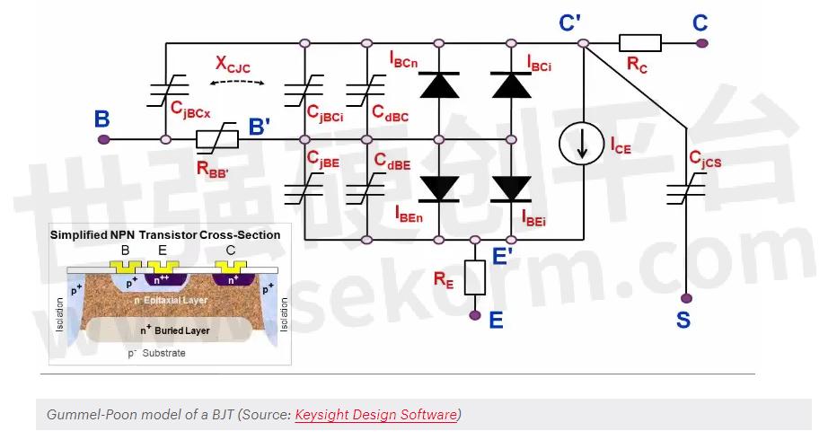
Such a model enables the following key capabilities among others:
· It gives equations for the currents in each region for I-V modeling.
· For C-V modeling, it gives equations for the junction capacitances.
· It enables accurate modeling over a variety of operating conditions by formulating physical phenomena like the Early effect of base-width modulation, the Webster effect, the Kirk effect, and more.
Device Model of a MOSFET
The illustration below is related to the physics-based device modeling of an n-channel MOSFET.
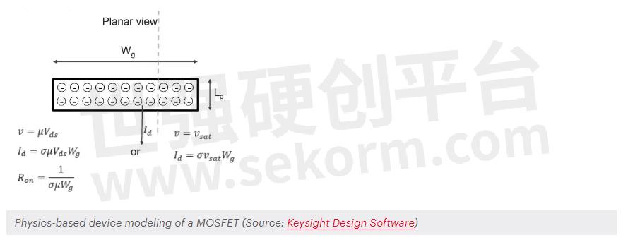
Such models use fundamental equations like Poisson's equation to determine characteristics like:
· Area charge density
· The electric field across the gate with an oxide insulator
Compact empirical models for MOSFETs — like the Berkeley short-channel IGFET model (BSIM) family — are based on these physics-based models. The BSIM models are optimized for fast circuit simulation and refined to fit real-world experimental measurements by adding parameters. They enable circuit designers to characterize MOSFET electrical behaviors using properties and parameters like:
· I-V and C-V characteristics
· Drain-source voltage, Vds
· Threshold voltage
· Gate capacitances
· Bulk threshold parameter
· Layer dimensions like the gate oxide thickness
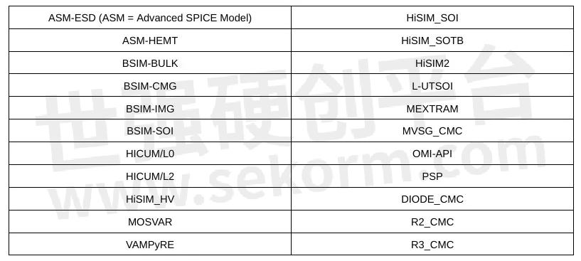
Standard Compact Models
Standardization of compact models enables all stakeholders to agree on the same modeling theories, equations, model parameters, mathematical attributes, definitions, and names. This facilitates the interoperability of different device designers, foundries, system integrators, and modeling/simulation software from different vendors.
The Compact Model Coalition (CMC) is a standards body that publishes a set of standard models for various devices. Some of the standard models are shown below.
Take a Look at KEYSIGHT’s Device Modeling Products and Services
Keysight offers a comprehensive set of EDA software and services for all stakeholders:
· PathWaveDevice Modeling (IC-CAP) is a keysight core, modular platform for device modeling.
· PathWave IC-CAP add-on packages add a variety of device models like GaN HEMT, GaN RF, power electronics, and more.
· PathWave Model Builder is a model extraction software with macro-modeling, Verilog-A support, and advanced fitting and optimization techniques.
· PathWave Model QA is a model validation tool.
· PathWave Advanced Design System is an advanced circuit design and simulation software with add-on bundles for specific analyses like electromagnetic, electro-thermal, or RF, and specialist industries like power electronics.
· PDKs of popular foundries are available for ADS.
In addition, Keysight provides device modeling services and special support services for EDA products.
- |
- +1 赞 0
- 收藏
- 评论 0
本文由雪飘梦飞转载自Keysight Blogs,原文标题为:An Introduction to Semiconductor Device Modeling,本站所有转载文章系出于传递更多信息之目的,且明确注明来源,不希望被转载的媒体或个人可与我们联系,我们将立即进行删除处理。
相关研发服务和供应服务
相关推荐

介绍模拟电路的仿真软件应用
ADS软件应用领域广泛,涵盖通信系统设计、卫星通信、毫米波雷达、汽车雷达和射频集成电路设计等领域。在通信系统设计中,ADS软件可用于优化无线通信系统的前端电路,提高信号传输质量和系统的性能。在卫星通信中,ADS可帮助工程师设计和仿真卫星通信链路,提升传输效率和系统性能。在毫米波雷达和汽车雷达领域,ADS的仿真和分析功能有助于提高雷达系统的探测精度、抗干扰性和可靠性。

什么是X参数?X参数和S参数有什么区别?
本文以 ADS 软件电路仿真为例,由 Hot S22 引入了 X参数的概念;并介绍了 X 参数的实验设计,使用 ADS电路仿真,通过三次不同的仿真条件下得到的结果进行运算得到 X参数中的几个分量,并于 ADS软件直接提取的 X参数进行了对比。

是德科技解析ADS软件的功能和用途
为了设计高性能的电路并评估其性能,工程师需要使用先进的设计和仿真工具,ADS就是比较主流的一个软件。那么ADS是什么软件?ADS软件是干什么的?下面介绍一下ADS软件的功能和用途。


如何在ADS中进行通道仿真?
在评估高速通道的性能时,过去经常采用瞬态仿真(Transient simulation)来查看接收端的时域特性,但是随着信号速率的不断增加,我们需要考虑的因素越来越多,或者说之前不起眼的因素会对我们的信号质量产生严重的影响。为了解决上述问题,KEYSIGHT推出了通道仿真解决方案,这篇文章就来学习如何在ADS中进行通道仿真,以及通道方针所涉及的一些问题。

【经验】想要制作自定义的ADS设计套件吗?先来看看ADS原理图元件库的制作过程
ADS是工程师用于各种高频和高速电路与系统设计应用的主力工具,覆盖芯片,模块,板级设计,要使用该设计环境并利用其仿真功能,设计人员应具有链接到模型文件或仿真数据的元件库,设计套件即是以设计师为本的元件库工具包。本文介绍了自定义的ADS设计套件的过程。

是德科技的PathWave ADS仿真软件,可以轻松仿真PCB串扰,加速产品开发流程
是德科技的PathWave ADS仿真软件,可以轻松仿真PCB串扰,结合是德科技的网络分析仪和PLTS软件进行串扰的测试,可以完成从概念设计、仿真、原型机设计、验证到生产制造和部署的全流程管理,从而加速产品开发流程。

【应用】Keysight ADS CILD和SIPro助力PCIE 5.0设计layout前后验证
本文主要介绍了PCIE 5.0主要指标、PCIE 5.0 设计面对的挑战、应对PCIE5.0设计挑战和PCIe 5.0仿真实例;突出了是德科技在开发中所提供的完美解决方案优势,针对于PCIE 5.0 设计面对的挑战,在Keysight ADS中,CILD和SIPro两个工具,可以分别满足PCIE 5.0 设计 layout前后的验证要求。

ADS与PCB协同仿真?是德科技的ADS软件成最主流的仿真工具
在进行射频PCB电路设计的时候,我们一般靠“经验”和“原则”指导设计,某些情况经验的作用也是有限的。要设计好射频板级电路,仿真是必不可少的。之所以某些经验可以替代仿真,是因为产品的电路非常成熟或集成化程度较高,对于创新型的设计,单纯依赖经验往往是不够的。科学的方法是将PCB封装和元器件仿真模型进行Co-Simulation半实物仿真,是德科技的ADS软件是最主流的仿真工具。

接口总线标准的仿真设计与测试技术发展趋势
高速数字电路设计与测试技术发展近十多年来,数字集成电路和各种接口总线标准的发展令人眼花缭乱,目不暇接。各个总线标准通常由不同团队制订,其纷繁芜杂的测试和测量技术给从业人员带来许多困扰。本文将就当下的一些主要接口总线标准的仿真设计与测试技术发展趋势作一些简明的总结和说明。

【经验】基于是德科技PathWave SystemVue的IBIS AMI建模方案详解
目前市场上能提供AMI模型建立以及测试工具的厂商很少,是德科技的PathWave SystemVue以及PathWave ADS(Advanced Design System)是目前市场上被广泛采用的工具。

【应用】Keysight ADS提供通用的PAM4 PRBS源和TX/RX模型助力光模块设计与仿真
Keysight ADS提供通用的PAM4 PRBS源和TX/RX模型助力光模块设计与仿真技术,本文介绍了高速光模块的电路设计与仿真。

如何在ADS中进行通道仿真
为了解决这些问题我们就必须采用一些均衡(EQ)措施,或者采用编码等方法。此外,由于处理的数据量增加,瞬态仿真非常的耗时间,这样看来瞬态仿真就显得力不从心了。为了解决上述问题,Keysight推出了通道仿真解决方案,学习如何在ADS中进行通道仿真,以及通道方针所涉及的一些问题。

是德科技电磁仿真软件RFPro成功验证支持Intel Foundry的Intel 18A工艺技术
是德科技宣布,RFPro电磁(EM)仿真软件作为是德科技EDA先进设计系统(ADS)综合工具套件中的一员,现已通过Intel Foundry认证,可帮助设计工程师开发采用Intel 18A工艺技术的设计。射频集成电路(RFIC)设计团队可结合使用这一全新的EM仿真功能和用于Intel 18A电路和物理设计的工艺设计套件(PDK),一次性设计出成功的产品。

是德科技解析ADS软件和射频电路仿真
Keysight PathWave先进设计系统(ADS)通过将互连电路设计软件的模块――包括射频集成电路(RFIC)、单片微波集成电路(MMIC)、层压板、晶圆级封装、天线和印刷电路板(PCB)――智能集成到密集的3D结构中,可以大幅减少代价高昂的硬件故障。根据具体应用,您应该选择合适的软件。

电子商城


现货市场

服务
提供是德(Keysight),罗德(R&S)测试测量仪器租赁服务,包括网络分析仪、无线通讯综测仪、信号发生器、频谱分析仪、信号分析仪、电源等仪器租赁服务;租赁费用按月计算,租赁价格按仪器配置而定。
提交需求>
朗能泛亚提供是德(Keysight),罗德(R&S)等品牌的测试测量仪器维修服务,包括网络分析仪、无线通讯综测仪、信号发生器、频谱分析仪、信号分析仪、电源等仪器维修,支持一台仪器即可维修。
提交需求>
授权代理品牌:集成电路


授权代理品牌:分立元件


授权代理品牌:接插件及结构件


授权代理品牌:部件、组件及配件


授权代理品牌:电源及模块


授权代理品牌:电子材料


授权代理品牌:仪器仪表及测试配组件


授权代理品牌:电工工具及材料


授权代理品牌:机械电子元件


授权代理品牌:加工与定制


登录 | 立即注册
提交评论