3PEAK Introduced Ultra-low Power Devices TPA5512 and TP2112 to CGM Solution, Supporting Rail-to-rail Input and Output


Traditional Blood Glucose Monitors (BGMs) involve frequent finger pricking for blood samples, causing discomfort and posing a potential risk of infection. Moreover, BGMs have blind spots for glucose monitoring and cannot effectively monitor glucose levels at night. While these issues may be manageable for patients with type 2 diabetes, they are significantly more troublesome for those with type 1 diabetes.
To address these challenges, CGMs have emerged. CGMs greatly improve upon two key issues found with traditional BGMs. By utilizing a subcutaneously implanted sensor, they offer a compact and comfortable solution. CGMs can continuously monitor glucose levels for 7 to 14 days. A common product design is shown in the picture below.

3PEAK Products for CGM Applications
Glucose measurement in CGMs is based on extracting glucose from the blood, which reacts with glucose oxidase on test strips to generate a measurable current. These products are typically powered by a single button cell battery, requiring at least two weeks of continuous operation. This necessitates a high demand for low power consumption in the built-in device.
Ultra-Low Power Operational Amplifiers
CGM devices are categorized into integrated Analog Front Ends (AFEs) and discrete solutions. The latter requires an operational amplifier for I-V conversion amplification and to apply an excitation power source, facilitating a current flow induced by an enzymatic reaction. The current generated by this reaction typically ranges from a few nanoamps to tens of nanoamps, necessitating an operational amplifier with an Input Bias Current (Ibias), paired with megaohm-level I-V conversion resistors. Considering battery life, power consumption needs to be minimized. Additionally, due to the product's compact size, a smaller package is preferred. Depending on the electrode configuration, operational amplifiers typically require two to four channels.
For varying resolution requirements, 3PEAK recommends its ultra-low power devices TPA5512 and TP2112, both supporting rail-to-rail input and output. The TPA5512 device consumes only 650-nA, has a maximum Offset Voltage (Vos) of 30-μV, a temperature drift coefficient of 0.025-μV/°C, and an Ibias of only 20-pA, making it highly suitable for precise CGM applications. It supports a supply range as low as 1.7-V, catering to 1.8-V battery-powered applications. Notably, TPA5512 offers various package options (SOIC-8, MSOP-8, and DFNX2-8), with the DFN package being ideal for space-sensitive applications. If the requirements for Vos are moderate (for instance, calibrated through software), the TP2112 device can be considered. It has a power consumption of only 500-nA and an Ibias as low as 1-pA. Available in SOIC-8 and MSOP-8 packages, it offers exceptional value for applications.
TPA5512 Specifications
Power Supply Range: 1.7 V to 3.6 V
Number of Channels: 2
Typical Quiescent Power: 650 nA
Maximum Vos: 30 μV
Temperature Drift Coefficient of Vos: 0.025 μV/°C
Typical Ibias: 20 pA
Bandwidth and Slew Rate: 9 kHz and 3 mV/μs
Noise Indicator: 354 nV/√Hz @ 100Hz
Package: SOIC-8, MSOP-8, DFN2X2-8
TP211x Specifications
Power Supply Range: 1.8V to 5.5V
Typical Quiescent Power: 500 nA
Maximum Vos: 1.5 mV
Temperature Drift Coefficient of Vos: 0.4 μV/°C
Typical Ibias: 1 pA
Bandwidth and Slew Rate: 10 kHz and 6 mV/μs
Package: SOIC-8, MSOP-8
As batteries deplete during use, their output voltage decreases. A boost device is necessary to stabilize voltage output and extend battery life. The introduction of batteries as low as 1.5-V has made boost devices even more essential for powering MCUs.
The TPQ05100 ultra-low-power boost chip from 3PEAK is a synchronous boost converter suitable for low-voltage systems. With an input voltage range of 0.9-V to 5.5-V, it can support even lower input voltages. The output voltage is adjustable from 2.5-V to 5.5-V. Its unique small packages, QFN2X2-6 and WLCSP (0.8 mm × 1.2 mm), are highly suitable for space-constrained applications.
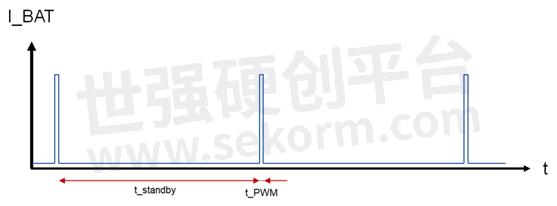
Due to the continuous dormancy of CGM for the majority of time, it only operates intermittently at a fixed frequency. This implies that the battery-powered load operates in PWM form rather than in a continuous mode, as illustrated below.

The device is in sleep mode for over 99% of the time, necessitating a high demand for efficient quiescent current to extend battery lifespan. During this time, the load is minimal, measured in microamperes, but spikes to milliampere levels for less than 1% of the time. Such high-current pulses often result in significant surge currents, affecting battery capacity and longevity. The TPQ05100 includes an internal current-limiting circuit to effectively reduce surge currents during these pulses, thereby enhancing battery life. Despite the pulses lasting only milliseconds, including pulse setup and sampling times, shortening these durations can significantly prolong battery usage. The TPQ05100's rapid transient response efficiently minimizes pulse setup times, leading to faster sampling and reduced current consumption.
TPQ05100 Specifications
Power Supply Range: 0.9 V to 5.5 V
Output Range: 2.5 V to 5.5 V (fixed output versions available)
Maximum Output Current: 600 mA
Typical Quiescent Current: 260 nA
Package: WLCSP-6, DFN2X2-6
Ultra-Low Power Low Dropout Regulator (LDO)
The battery's voltage output fluctuates significantly. Directly powering operational amplifiers from the battery can affect their output precision. For this scenario, 3PEAK recommends its ultra-low power LDO, the TPL710. This low-voltage LDO boasts an extremely low quiescent current and quick response to dynamic loads. It stabilizes with just a 2.2-μF ceramic capacitor and features current limiting and over-temperature protection, significantly improving product reliability. With EN control, it outputs fixed voltages between 1.0-V and 3.6-V, available in various packages, including SOT23-3, SOT23-5, and the compact DFN1X1-4.
TPL710Fxx Specifications
Power Supply Range: 2.4 V to 6.0 V
Maximum Output Current: 200 mA
Typical Output Accuracy: 1%
Typical Quiescent Current: 1.4 μA
Dropout Voltage: 170 mV @ 200 mA
PSRR: 54 dB @ 1 kHz
As the number of patients with diabetes continues to increase each year, the demand for comfortable CGM devices is also on the rise. These devices, with their unique medical attributes, require both measurement accuracy and reliability. 3PEAK, with years of dedication in the signal chain and power supply domains, leads in performance and strict quality control. Boasting a comprehensive delivery system and partnerships with key domestic healthcare clients, 3PEAK is a trusted partner you can rely on.
- |
- +1 赞 0
- 收藏
- 评论 0
本文由上山打老虎转载自思瑞浦 微信公众号,原文标题为:Ultra-Low Power, High Precision, Compact Size! 3PEAK's Continuous Glucose Monitoring System (CGM) Solution,本站所有转载文章系出于传递更多信息之目的,且明确注明来源,不希望被转载的媒体或个人可与我们联系,我们将立即进行删除处理。
相关推荐
3PEAK Announces High-Voltage LDO TPL8031Q Featuring Auto-Grade 3-μA Ultra-Low Static Power Consumption
TPL8031Q has a shutdown current of less than 1μA, with a typical quiescent current of only 3μA. Its low power consumption mode performs exceptionally well, making the regulator particularly suitable for various applications with high requirements for standby power consumption, such as rain-sensing wipers and automatic headlights.
3μA超低静态功耗!思瑞浦推出汽车级超低静态功耗高压LDO TPL8031Q,输出电容1~200μF
思瑞浦3PEAK推出全新一代汽车级超低静态功耗高压线性稳压器——TPL8031Q,拥有支持3V~42V宽输入电压范围、3μA超低静态功耗、多种封装可选等性能优势,可广泛应用于汽车12V电池供电、待机低功耗的各种汽车应用场景。
思瑞浦(3PEAK)运算放大器选型表
思瑞浦(3PEAK)高性能运算放大器,精密运算放大器:失调电压低至5uV,温漂低至0.008uV,支持双电源供电。低噪声运算放大器:噪声系数低至0.1μVpp/Hz,适用于低噪声系统应用。超低功耗运算放大器:功耗低至300nA,轨到轨输出,适用于电池供电产品。超低功耗比较器:功耗低至300nA。负载驱动电流25mA,适用于便携式设备。
|
产品型号
|
品类
|
Status
|
Rating
|
Package
|
Channel
|
Supply Voltage(Min)
|
Supply Voltage(Max)
|
Iq per channel (Max)(μA)
|
GBW (Typ) (MHz)
|
Slew Rate(Typ)(V/μs)
|
Rail-Rail In
|
Rail-Rail Out
|
Ishort(Typ) (mA)
|
Vos(Max)(mV)
|
Offset Drift(Typ)(μV/°C)
|
Ib(typ)(pA)
|
Vn (Typ) (nV/rtHz)
|
Peak Noise at 0.1 to 10Hz(μVpp)
|
Operating Temperature Range(°C)
|
|
LM2904A-VR
|
高压运算放大器
|
Production
|
Industrial
|
MSOP-8
|
2
|
3
|
36
|
200
|
0.9
|
0.5
|
No, to V- only
|
Yes
|
30
|
3
|
7
|
60
|
70
|
20
|
-40 to 125
|
选型表 - 思瑞浦 立即选型
思瑞浦(3PEAK)线性稳压与基准选型表
低压差、高PSRR,低功耗,低噪,最大输出电流(mA):150~3000,更有DDR端供电专用LDO,具有灌、拉电流能力。
|
产品型号
|
品类
|
Status
|
Rating
|
Package
|
Maximum Output Current(mA)
|
Iq(mA)
|
PSRR @1KHz (dB)
|
Dropout(mV)
|
Input Voltage(V)
|
Accuracy(max)
|
Noise(μVRMS)
|
|
TPL503133-S5TR
|
LVLDO
|
Production
|
Industrial
|
SOT23-5
|
300
|
0.055
|
70
|
250
|
1.5~5.5
|
±2%
|
178
|
选型表 - 思瑞浦 立即选型
思瑞浦LDO效率如何?
LDO的转换效率主要取决于输入电压VIN和输出电压VOUT的比例,当输入电压和输出电压之间取低压差时会取得较高效率,当负载电流较大时效率大约是VOUT/VIN。
TPL930 Series 3-A Output, High-PSRR, Low-Noise LDO Regulator
型号- TPL930,TPL930 SERIES,TPL930ADJ-QF6R
思瑞浦(3PEAK)DC-DC转换器选型表
工业级,应用温度范围-40 to +125℃;宽压降压转换器:输入电压3V~60V,输出电压0.6V~100V;中压降压转换器:输入电压 4.5V~17V,输出电压0.6V~17V;低压降压转换器:输入电压2.8V~6V,输出电压0.8V~17V;升压转换器:输入电压0.9V~80V,输出电压VIN~80V。
|
产品型号
|
品类
|
Status
|
Rating
|
Package
|
VIN(V)
|
Output(V)
|
Max Output Current(A)
|
Switching Frequency (kHz)
|
|
TPP60308-ES1R-S
|
宽压降压转换器
|
Production
|
Industrial
|
ESOP8
|
4.5~60
|
0.8~60
|
3.5
|
100-2500
|
选型表 - 思瑞浦 立即选型
思瑞浦LDO的输入电压范围为多少呢?
输入电压范围看不同的产品型号,高压LDO一般支持到最高42V正常工作范围,可以作为车载一级电源;思瑞浦也有5V-6V最大输入电压的低压LDO产品系列和~20V最大输入电压的中压LDO产品,提供完整的产品矩阵。
TPL9032 Series 300-mA High PSRR, Ultra-low Noise LDO
型号- TPL9032 SERIES,TPL903230-S5TR,TPL903228-DF1R,TPL903225-DF1R,TPL903236-S5TR,TPL903231-WS1R,TPL903225-S5TR,TPL903233-DF1R,TPL903228-S5TR,TPL9032285-WS1R,TPL903230-DF1R,TPL903233-S5TR,TPL90321875-WS1R,TPL9032XX-WS1R,TPL903231-DF1R,TPL903229-DF1R,TPL9032XX-S5TR-S,TPL9032,TPL903245-S5TR,TPL903218-DF1R,TPL903229-S5TR,TPL903212-S5TR,TPL903218-S5TR,TPL9032XX-DF1R,TPL903215-S5TR,TPL903212-DF1R,TPL903225-WS1R,TPL903233-WS1R,TPL903218-WS1R
【选型】思瑞浦线性稳压LDO TPL820用于网关项目,输出电压1.2V~5V,具有多种型号可选
在网关项目中,有需要用到输出3.3V,输出电流150mA的LDO,这里选用了思瑞浦推出的线性稳压LDO TPL820系列中的TPL820F33-3TR,具有固定输出电压3.3V,输出电流180mA。
思瑞浦LDO产品有哪些电压输出?
LDO有可调电压输出版本和固定电压输出版本。可调输出电压版本可以通过板外分压电阻来设置输出电压;固定电压输出版本一般会覆盖5V、3.3V、1.8V等常见电压点。
TPL710 200mA output, 1 μA Ultra-Low Quiescent Current LDO DATA SHEET
型号- TPL710F25-FR,TPL710F25-89TR,TPL710F30-89TR,TPL710F10-3TR,TPL710F28,TPL710F2-5TR,TPL710F33-89TR,TPL710F25,TPL710F10-5TR,TPL710F28-89TR,TPL710F10,TPL710F30,TPL710F33-5TR,TPL710F28-3TR,TPL710F33-3TR,TPL710F30-FR,TPL710F12-5TR,TPL710F25-3TR,TPL710F12-3TR,TPL710F28-FR,TPL710,TPL710F18-89TR,TPL710F18,TPL710F12,TPL710F12-89TR,TPL710F33,TPL710F25-5TR,TPL710F18-3TR,TPL710F30-3TR,TPL710F18-5TR,TPL710F10-89TR,TPL710F30-5TR,TPL710F18-FR,TPL710F33-FR,TPL710F12-FR,TPL710F10-FR
如果定义Vin_max<10V的LDO为低压LDO,Vin_max≤30V的LDO为中压LDO,Vin_max≤42V的LDO为高压LDO,则哪款低压LDO更合适?
推荐思瑞浦(3PEAK) 车规级 TPL910Q,具有78dB的PSRR,4.9μVrms的噪声,0.8-5V的可调输出电压,可以灵活设置,具有1A的大电流输出,在输出电流为1A时有500mV的低压降:https://www.sekorm.com/news/57339338.html
【经验】在输出电流防反灌电路中应用思瑞浦LDO的设计注意事项
某客户设计一款吸尘器,应用3PEAK的LDO TPL730,但是负载并不是普通的阻性负载,实际应用为给电容做充电电源,负载为容性负责,因为电容属于储能装置,所以在关断LDO时会出现电流反向流入输入的情况,本文主要帮助客户设计一种防反灌电路。
【选型】国产2A电流LDO芯片TPL920对比TI的TPS7A8300,可兼容设计
通信基站项目中,为后级供电的2A电流LDO芯片,许多设计原先采用TPS7A8300,在目前芯片短缺形势下,为了预防采购问题导致的生产难题,需要做国产化设计。本文对TI的TPS7A8300和3PEAK(思瑞浦)的TPL920做一个参数对比,说明两者兼容,为设计者提供参考。
电子商城
现货市场
服务
可贴片PCB尺寸50*50mm-580*610mm;PCB厚度0.3-8mm;贴装精度CHIP元件+0.03,BGA Pitch 大于0.25mm;元件尺寸0201-74*74BGA;元件高度:30mm。
最小起订量: 1 提交需求>
可定制LAMP LED、 CHIP LED、 PLCC LED、 汽车用车规级LED、COB LED的尺寸/电压/电流等参数,电压1.5-37V,电流5-150mA,波长470-940nm。
最小起订量: 30000 提交需求>


登录 | 立即注册
提交评论