MULTI-PROTOCOL USB: An All-Serial Data Acquisition System – No Microcontroller Required!


Introduction
The vast majority of USB devices available on the market today have at least one thing in common; they all use microcontrollers to implement the task at hand. Whether it’s in the form of a USB serial engine sharing the same piece of silicon with a microcontroller or a simple connection between the two on a printed circuit board, the use of a microcontroller for just about any USB-based task is virtually inescapable…that is, until now.
In the arena of "easily-implemented USB", the folks at FTDI have done it yet again by releasing their new, dual-channel FT2232C IC. This new chip offers two interfaces for connection to user electronics as compared to its predecessors (the FT232BM and FT245BM) that only have one. Instead of being fixed in hardware as only serial (USB-UART) or parallel (USB-FIFO), both channels of this new chip are configurable for either serial, parallel, or one of several other new interface modes of operation.
This article will focus on one of the new interface modes known as the “Multi-Protocol Synchronous Serial Engine” or MPSSE for short. The MPSSE interface is only available on one of the two channels and consists of a clock line, a data IN line, a data OUT line, and some general-purpose digital I/O lines. The MPSSE can be controlled via any programming language with the ability to open, load, and access a Dynamically Linked Library (DLL). I wrote my program in Visual C++ to demonstrate the MPSSE, but Visual Basic and other programming languages can be used as well. (We’ll talk more about software later…)
I will further demonstrate how to use the MPSSE to communicate with a 12-bit A/D converter, a 12-bit DAC, 12 digital I/O lines, and control 4 relays, all without the use of a microcontroller…and all without any in-depth knowledge of USB!
Hardware Design
A printable version of the schematic (Figure 1) is available for download as a *.pdf document from www.dlpdesign.com/usb/2232daq/ .
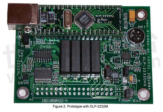
A picture of the prototype printed circuit board is shown in Figure 2. The picture shows the prototype using the DLP-2232M, but it could be used with either the DLP-2232M or DLP-2232ML dual-channel USB interface modules.
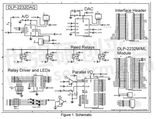
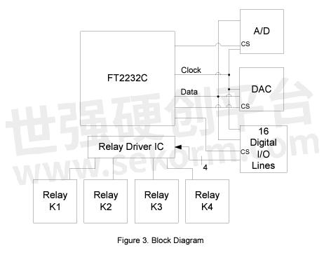
The data-acquisition devices used in this design all have serial interfaces; perfect for use with the MPSSE. The data IN and data OUT lines of the MPSSE are connected at the DLP-2232M(L) interface to form a single, bi-directional data line. This data line and the clock line are shared between all of the acquisition devices in the design, and each device is enabled for communication via one of the general-purpose digital I/O lines on the FT2232C.
Figure 3 shows a simplified block diagram of the data acquisition system.
The A/D is a dual-channel, 12-bit, successive-approximation converter that was chosen for its low cost and small size. The intention of this hardware design was more to show off the capabilities of the MPSSE and less to provide a large-scale or highly accurate data acquisition system. That said, 12 bits (1.2-millivolt resolution) is likely to be more than enough for most voltage measurements on the 0-5 volt range.
Since the voltage reference for this converter is tied to the VDD line internally, VDD is the reference and can be any value from 4.5-5.5 volts. Since this A/D is communicating digitally with a 5-volt system, taking VDD below 4.5 volts could cause damage and would definitely affect accuracy. In this design, the VDD line for the converter is brought out to the interface header via J2, and either the 5-volt supply from the USB port can be used or an external voltage provided through H1. For most applications, the 5-volt power from the USB port should work just fine.
The DAC employed in this design is also a 12-bit, dual-channel device that has its reference voltage pin brought out to interface Header H1. If Jumper J3 is set to positions 1 and 2, the output voltage range will be from 0 to approximately 5 volts or whatever the voltage is currently on the USB port. If Jumper J3 is set to positions 2 and 3, then an external reference can be used in the range of 0-5 volts. For example, if an external voltage reference of 2 volts is used, then the output voltage range of the DAC will be 0-2 volts with a resolution of 490 microvolts (2.0/4096).
The chip used to implement the 12-bit digital I/O bus (also referred to as an I/O Expander) is a Microchip MCP23016, and it can have each of its I/O lines configured as either input or output. Since the I/O Expander does not have a chip select line, an external buffer (U3) was used to prevent the clock line from initiating a reply on the data line while the MPSSE is communicating with another device.
The four relays used in this design are SPST reed relays, and they require very little current (10mA) to energize their internal 5-volt coil--perfect for USB port-powered applications. They do not need internal protection diodes since the ULN2003A already has the protection diodes built in. When the MCP23016 first powers up, its I/O pins are set to input, so 100K pull-down resistors were added to ensure the relays would all be off.
FT2232C
The best source of information on the FT2232C is, of course, the datasheet. To briefly summarize some of its high points, the two channels of the chip can be individually configured to use either the Virtual COM Port drivers (these make the port look like an RS232 serial port to the host application) or the DLL drivers. Each channel can be configured for any of the various modes of operation (MPSSE is only available on Channel A), and these selections are made via writing to an EEPROM device that is connected to the FT2232C.
Other new modes of operation for this device are Synchronous Bit-Bang Mode, a CPUstyle FIFO Interface Mode, MCU Host Bus Emulation Mode, and Fast Opto-Isolated Serial Interface Mode. Additionally, a new high-drive level option means that the device UART/FIFO IO pins will drive out at around three times the previous power level, meaning that the bus can be shared by several devices. Classic BM-style Asynchronous Bit-Bang Mode is also supported, but it has been enhanced to give the user access to the device’s internal RD# and WR# strobes.
Both channels of the FT2232C are “full-speed” USB devices, but since there is only a single connection to the host, the combined data throughput for both Channels A and B will not exceed a maximum of about 8 megabits per second.
The true power of the chip is perfectly illustrated when both channels are used in a design in which a programmable device is reconfigured in real time “on the fly”. One example of this would be an FPGA configured via the MPSSE on Channel A. Once configuration is complete, Channel B is then used to communicate with the FPGA at full speed. Another example would be using the MPSSE to write hex program data to the Flash program memory area of a microcontroller with Channel B communicating with the micro at run-time.
Programming
As mentioned earlier, to enable and access the MPSSE, you must use FTDI’s DLL drivers. Visual C++ demo source code that demonstrates the use of the DLL is available for download from www.dlpdesign.com. Using the MPSSE requires the use of a programming language that can open and access a DLL at run-time. The first step in using the DLL is to open the DLL and load the functions. The application will only be able to do this if the DLL drivers have been loaded onto the computer, and the drivers can only be loaded by connecting an FT2232C USB chip to the computer. Once the drivers are properly loaded, the attached USB chip will appear in Device Manager under “Universal Serial Bus Controllers”.
Once the DLL drivers are opened and loaded, simple function calls are used to open a communications port and enable the MPSSE. To use the MPSSE, you begin by setting the speed at which the MPSSE will clock out data. You then select a clock/data scheme that works with the connected hardware. In the case of our A/D converter, we want commands to be clocked in and conversion results to be clocked out on the rising edge of the clock. MPSSE commands 0x13 and 0x20 will accomplish these tasks. (FTDI App. Note AN2232C-01 outlines all of the features of the MPSSE and is available for download from dlpdesign.com or ftdichip.com.) Since the MPSSE uses a rather low-level coding method, adding comments to your code is key to understanding what you’ve done the next day when you look at the code again.
Before the MPSSE can communicate with the A/D, its chip select line (ADCS) must be enabled by taking it low. This is accomplished with the command 0x80. Following is a short code example (with comments!) for enabling communications and performing a single read of the A/D converter:
//take ADCS low
pos=0;
tx[pos++] = 0x80;//Setup MPSSE Low byte I/O lines
CLEAR(LowByteHiLowState, ADCS);//macro for clearing a bit
CLEAR(LowByteHiLowState, CLKSTATE);//start with clock low
tx[pos++] = LowByteHiLowState;
tx[pos++] = OUTPUTMODE;
//send control nibble to ADC
tx[pos++] = 0x13; //Clock out bits, MSB first
tx[pos++] = 0x03; //3 = 4bits
tx[pos++] = AD1; //1111 Start, SnglCh, Ch1, MSBF
//set data direction of AD1 to input
tx[pos++] = 0x80;//Setup MPSSE Low byte I/O lines
tx[pos++] = LowByteHiLowState;
tx[pos++] = INPUTMODE;
//read 2 bytes from A/D conversion
tx[pos++] = 0x20;//Clock out data, MSB first
tx[pos++] = 0x01;//LengthL 0=1byte, 1=2bytes
tx[pos++] = 0x00;//LengthH
//this results in 2 bytes appearing in the RX buffer
//take ADCS back high
tx[pos++] = 0x80;
SET(LowByteHiLowState, ADCS);//take ADC enable high
tx[pos++] = LowByteHiLowState;
tx[pos++] = OUTPUTMODE;
//send the command string Write(tx, pos, &ret_bytes);
The idea is to build a long stream of commands that can be processed at high speed by the MPSSE and send them all at once. The MPSSE will process the entire string of commands at a preset rate and return the data requested by that string of commands (if any) to the data buffer on the host that was created when the port was opened.
DO-RE-MI Whistle Control
By now you have likely seen the microphone and preamp circuit (Figure 4) and are wondering, “What am I supposed to do with that?” Well, now that we have an A/D converter and an MPSSE that allows us to sample voltages at a known rate, I thought I’d make a listening device that could not only hear someone whistling 30 feet away but also calculate the frequency of the note that was being whistled using an FFT and perform a specific operation based upon that note. For example, every time you whistle the note for ‘DO’ (Remember that movie, the Sound of Music? Now I’m showing my age…) and hold it for one second, toggle the state of Relay K1 to turn on or turn off a fan. Or, when you whistle the note for MI, take digital I/O line P01 high, and then turn it off when you whistle the note for FA.
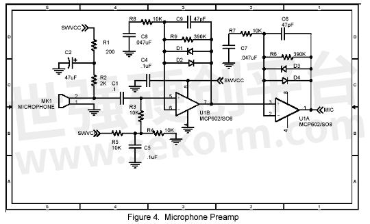
Since Middle C on a piano falls somewhere in the 260Hz range, you may want to jump up a couple octaves and use the note for C found at about 1040Hz. I doubt that anyone can whistle Middle C. Furthermore, if you whistle DO RE MI starting at 1040Hz, you may find it somewhat challenging to hit that last “TI” and “DO”. (I cheated a bit and started my DO RE ME at 840Hz so that I could comfortably whistle the entire scale--I’m sure Julie Andrews would be appalled!) Also, you don’t have to whistle the exact notes for DO, RE, and MI. Any note you can whistle from about 600Hz up to 2KHz can be 7 detected by this system due to the sample rate. Frequencies below 600Hz are ignored in the software since it’s almost impossible to whistle notes this low and these notes tend to appear more prominently in the audio spectrum when the room is otherwise quiet.
If you want to see just what range of frequencies your whistler can handle, download the FFT based screensaver from www.dlpdesign.com/usb/2232daq/ that listens to a microphone via the sound card in your PC and presents the frequency data in real time. (Keep in mind that you shouldn’t use this program as an actual “screen saver” because the frame around the image doesn’t change or move and will eventually burn the image onto your CRT.)
An FFT (Fast Fourier Transform) is a mathematical process that converts time domain information to the frequency domain and provides the unique ability to “listen” to each separate portion of the sampled audio spectrum with perfect clarity. If we acquire 128 voltage samples at a rate of 4,000 samples per second and an FFT is calculated, the result of the FFT is frequency domain data evenly divided up into 64 frequency “bins”. Each bin holds a single numeric value that represents the overall amplitude of that narrow range (bin) of frequencies.
OK, its time for some FFT rules:
The FFT is faster than its predecessor the DFT (Discrete Fourier Transform) in part because you must provide 2^n (32, 64, 128, etc.) number of input samples.
2. Thanks to work performed back in the 1920’s by Henry Nyquist, we know that the A/D must sample at a rate (known as the Nyquist frequency) that is twice that of the highest frequency we are expecting to find in the frequency domain in order to properly acquire the signal.
3. If the analog signal being sampled has frequency components that are higher than half the sampling rate, then an anti-aliasing filter must be used to filter out these frequencies or the resulting FFT output data will be flawed. A filter of this type is typically a low-pass filter fashioned out of op amps, resistors and capacitors.
4. The resulting number of output bins equates to half of the number of input samples.
5. The number of data points taken--not the accuracy of the voltage measurement-dictates the resolution of the frequency domain data.
6. The accuracy of the frequency domain frequency data (i.e. not the amplitude data) is based on the accuracy of the A/D’s sampling rate.
For example : Let’s say our A/D is sampling at a rate of 4,000 samples per second and takes 128 voltage measurements from a signal that consists of a sine wave oscillating at 1,000Hz. If these 128 samples are number-crunched by an FFT, the result is 64 frequency domain data points or bins. Since we sampled at 4,000Hz, the maximum frequency that can be accurately acquired is 2,000Hz; and since a single 1,000Hz- signal was present in the source, then Bin Number 32 of the output data will hold a numeric value that is larger than all of the other bins.
There are other considerations that have been overlooked such as converting the data in the bins to usable power spectrum data (measured in dB) and using filters on the source data, but these items are beyond the scope of this article.
Now that we have access to frequency domain data and can detect which note is being whistled, all that is left to do is write an application that detects when a particular note (or a note within a specific range) has been held for a second or so and respond accordingly. A Windows application can be downloaded from dlpdesign.com that allows the user to set up these conditions and respond in a number of ways. (A screen shot of the program can be seen in Figure 5. Also, as mentioned earlier, source code for an example program that shows how to access the A/D, DAC, relays, and digital I/O lines is available for download.

Conclusion
There is a considerable amount of reading material available online (www.dlpdesign.com/pub.shtml ) for those wanting to become familiar with FTDI’s USB chips and drivers.
FTDI’s USB IC’s greatly simplify the task of designing a new product utilizing the increasingly popular USB interface, and the FT2232C builds upon that legacy by offering a configurable, two-channel version of their existing product line. FTDI’s USB drivers are quite mature (i.e. well debugged!) and are available for several operating systems.
Since the drivers are provided royalty free and a micro may not even be required for your application, it’s never been easier to hit the ground running with your new USB-based product design. Clearly, USB has a strong hold on the PC market and will remain available for the foreseeable future. Personally, I can’t imagine using any other interface!
- |
- +1 赞 0
- 收藏
- 评论 0
本文由wenxia转载自FTDI CHIP News,原文标题为:多协议USB:全串行数据采集系统 - 无需微控制器!,本站所有转载文章系出于传递更多信息之目的,且明确注明来源,不希望被转载的媒体或个人可与我们联系,我们将立即进行删除处理。
相关推荐

UC232R“ChiPi”最小组件FT232RL USB至RS232转换器电缆
描述- 该资料介绍了FTDI公司的UC232R“ChiPi”最小组件USB到RS232转换电缆。它集成了FT232RL USB-串行UART接口IC设备,具有时钟发生器输出和FTDIChip-ID™安全启动盘功能。该电缆支持异步和同步位打接口模式,并简化了外部EEPROM、时钟电路和USB电阻的集成。
型号- FT232RQ,FT2232C,FT232R,ZT213LEEA,UC232R,FT232RL
Morph-IC数据表1.0版
描述- MORPH-IC是一款结合了FTDI的FT2232C USB接口集成电路和Altera ACEX 1K系列FPGA(EP1K10TC100-3)的紧凑型模块。该模块具有灵活的USB接口,支持快速编程/重新编程FPGA,适用于仪器、通信和其他需求严格的领域。
型号- D2XX,EP1K10TC-100,FT2232C,FT2232,EP1K10TC100-3,MORPH-IC

FTDI集成电路器件RoHS2-2011/65/EU和(EU)2015/863符合性声明(FT_000223))
型号- FT245BM,FT2232D,FT2232C,FT8U100AX,FT8U232AM,FT245BL,FT232BM,FT232BL,FT8U245AM
UM232R USB-串行UART开发模块数据表
描述- UM232R是一款基于FTDI FT232RL芯片的USB到串行UART开发模块。该模块支持多种数据传输速率,具有内置的3.3V电平转换器,适用于各种USB与串口之间的通信需求。
型号- FT232RQ,FT232R,FT2232C,UM232R,FT232BM,FT232RL
MM232R USB-串行UART开发模块数据表
描述- 该文档为FTDI公司生产的MM232R USB-Serial UART开发模块的数据手册。该模块基于FT232RQ芯片,提供USB到串行UART接口功能,并集成了时钟发生器。它支持多种数据传输速率和波特率,适用于各种USB到串行的转换应用。
型号- FT232RQ,MIC2025-2BM,FT232R,FT2232C,MM232R,TC55,IRLML6402,FT232BM,FT232RL
FTDI RoHS2-2011/65/EU&(EU)2015/863符合性声明
描述- FTDI公司声明,其集成电路产品(除表2中列出的例外)符合欧盟2011/65/EU和(EU) 2015/863指令,即《关于在电气和电子设备中限制使用某些有害物质的指令》(RoHS2)。产品中不含有表1中列出的物质,且浓度不超过最大限制值。部分产品因不合规而提供替代品。
型号- FT245BM,FT2232D,FT2232C,FT8U100AX,FT8U232AM,FT245BL,FT232BM,FT232BL,FT8U245AM

如何区分USB Host 、USB Devices和USB HUB,一张图弄清楚USB分类
USB的英文缩写是UniversalSerialBus,中文就是“通用串行总线”,也称通用串联接口。Host就是主,可以起到控制作用;Device(slave)就是从,是被控制的。

FTDI CHIP FT4232HA在Embedded World 2022演示介绍 ∣视频
FTDI FT4232HA产品介绍。

特斯拉/苹果USB桥接芯片供应商FTDI Chip(飞特帝亚)授权世强硬创代理
FTDI Chip高速USB 2.0系列FT4232HA是业界首款USB 2.0高速转四通道UART或双通道MPSSE的车规级芯片。

FTDI CHIP的USB桥接系列产品选型表
通用串行总线 (USB) 现在已成为可靠,低成本数字链路与系统连接的接口。 USB的使用已经扩展到PC之外,现在可以在各种区隔市场中找到,包括工业,医疗,消费,通信,网络等等。 FTDI芯片能够让设计人员快速实现USB设计,提供全面的解决方案包括硅片,开发工具,应用笔记和软件支持。 凭借着USB桥接器的专业技术为各种接口(如 UART, FIFO, I2C, SPI, PWM 和 GPIO) 提供了无缝集成,桥接器将信号和协议从所选的接口转换为USB。提供多样的USB解决方案, 最小至3x3mm的10的DFN引脚封装形式,或模块形式可以直接插入主板进行开发和生产, 再或者用于USB桥接至众多接口的线缆。
|
产品型号
|
品类
|
速率(Mbit/kBit)
|
通道数量
|
接口
|
I/O 电压(V)
|
USB Host
|
封装
|
描述
|
|
FT232HPQ
|
USB高速PD IC
|
12MBit/s (UART) up to 40MBit/s (Sync FIFO)
|
1
|
UART, FIFO, 1 x MPSSE, Fast serial, CPU FIFO, Bit Bang/GPIO, FT1248
|
3.3V
|
No
|
QFN 56
|
单通道高速USB Type-C转多用途UART/FIFO/JTAG/SPI/I2C,带单PD端口
|
选型表 - FTDI CHIP 立即选型

FTDI芯片FT4232HA在Embedded World 2023演示介绍 ∣视频
FTDI FT4232HA demo板介绍。
FTDI CHIP的USB线缆选型表
FTDI CHIP的USB线缆选型表包含USB线缆、USB转USB零调制解调器线缆、USB TTL串行线缆和USB MPSSE线缆四个品类。USB速率(Gbps/Mbps)包含SuperSpeed (5Gbps)Full Speed (12Mbps)和High Speed (480Mbps)三种。USB 连接器有Type A和USB 3.0 Type A。
|
产品型号
|
品类
|
数据速率(Kbaud/Mbaud/mbps)
|
USB 连接器
|
终端连接器
|
线缆长度(m)
|
描述
|
|
CUB-100-BK
|
USB线缆
|
-
|
Type A
|
Micro Type B
|
1.0m
|
USB A转USB MICRO B 1M
|
选型表 - FTDI CHIP 立即选型
VM800P嵌入式视频引擎Plus模块的FTDI芯片VA800A程序数据表编程器
描述- VA800A PROG是一款用于VM800P Plus模块的程序器。它通过USB连接到PC,并通过SPI接口与VM800P Plus模块通信,实现对ATMEGA328P微控制器的编程。该程序器提供了一种替代内置USB至UART编程器的方案,并可用于恢复损坏或损坏的MCU。
型号- FT232RQ,VA800A-PROG,VA800A_PROG,VM800P,VA800A,ATMEGA328P,FT800

FTDI‘s IC FT60XQ USB 3.0 to FIFO Bridge ICs Products Are Used in Ultrasound Devices
Integrating FTDI chips into a medical ultrasound device would typically serve as a connection interface between the ultrasound machine and a computer or other digital device via USB. This bridge enables the transmission of ultrasound data from the machine to the computer for further analysis, storage or display purposes.

电子商城
品牌:FTDI CHIP
品类:Dual High Speed USB to Multipurpose FIFO IC
价格:¥38.3669
现货: 160
品牌:FTDI CHIP
品类:Dual High Speed USB to Multipurpose FIFO IC
价格:¥209.5419
现货: 0
品牌:FTDI CHIP
品类:Dual High Speed USB to Multipurpose FIFO IC
价格:¥43.4824
现货: 0
品牌:FTDI CHIP
品类:Dual High Speed USB to Multipurpose FIFO IC
价格:¥37.8750
现货: 0
品牌:FTDI CHIP
品类:High Speed USB Bridge with Type-C
价格:¥42.4987
现货: 0
现货市场
服务
支持GSM / GPRS 等多种制式产品的射频测试,覆盖所有上行和下行的各项射频指标,包括频差、相差、调制、功率、功控、包络、邻道泄漏比、频谱、杂散、灵敏度、同道干扰、邻道干扰、互调、阻塞等等。满足CE / FCC / IC / TELEC等主流认证的射频测试需求。
实验室地址: 深圳 提交需求>
可烧录MCU/MPU,EPROM,EEPROM,FLASH,Nand Flash, PLD/CPLD,SD Card,TF Card, CF Card,eMMC Card,eMMC,MoviNand, OneNand等各类型IC,IC封装:DIP/SDIP/SOP/MSOP/QSOP/SSOP/TSOP/TSSOP/PLCC/QFP/QFN/MLP/MLF/BGA/CSP/SOT/DFN.
最小起订量: 1 提交需求>
授权代理品牌:集成电路


授权代理品牌:分立元件


授权代理品牌:接插件及结构件


授权代理品牌:部件、组件及配件


授权代理品牌:电源及模块


授权代理品牌:电子材料


授权代理品牌:仪器仪表及测试配组件


授权代理品牌:电工工具及材料


授权代理品牌:机械电子元件


授权代理品牌:加工与定制


登录 | 立即注册
提交评论