UV Lasers from Coherent Enable Detection of Minute Defects on Semiconductor Wafers




UV lasers from COHERENT enable detection of minute defects on semiconductor wafers which is key to maximizing yields and lowering cost.

The Apollo Guidance Computer (AGC) used by NASA for the moon landing cost approximately $150 million when it was built in the 1960s ($1 billion in today’s dollars). It was about the size of a microwave oven and weighed around 32 kg.
Today, a top-of-the-line iPhone 15 costs $1600 and, of course, fits in the palm of your hand. And that iPhone is around 200 million times more powerful than the AGC in terms of the number of operations it can perform per second.
This increase in microprocessor power was predicted by Intel co-founder Gordon Moore, who stated that the number of transistors on a microchip would double approximately every two years. But the comparison just cited also highlights an important corollary to Moore’s Law, sometimes called Moore’s Second Law. Namely, that the amount of microprocessor power available per dollar also increases exponentially over time.
Both Moore’s First and Second Laws have remained true over time because the semiconductor industry has simultaneously focused on achieving two different goals. The first is to make circuit elements and assemblies smaller. The second is to relentlessly lower costs.
A critical cost factor in semiconductor fabrication is yield, and one significant factor affecting that is defects and contaminants in the production environment. To reduce defects, manufacturers make substantial investments in equipment, such as cleanroom environments, to prevent contamination from the outset. Additionally, they deploy advanced inspection techniques to detect and minimize the impact of any defects that do occur, ensuring optimal yields and cost efficiency.
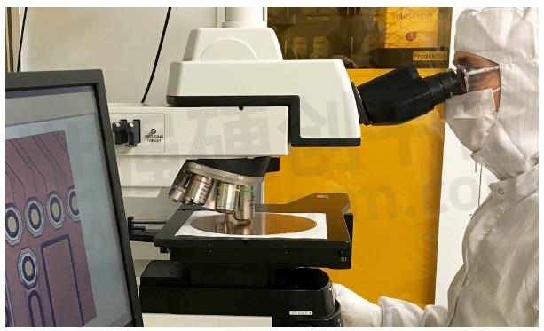
Lasers in Wafer Inspection
Lasers are an ideal tool for semiconductor inspection because they are a non-contact method that offers an unrivaled combination of sensitivity and speed. Furthermore, they’re highly versatile and can be optimized to perform a variety of different inspection tasks.
As a result, lasers have been used for inspection since the very early days of the microelectronics industry. In the late 1960s – not long after lasers were first introduced into the market – they were already being employed for metrology tasks, such as measuring wafer flatness and thickness.
In the 1980s, as semiconductor devices became smaller and more complex, the industry began to adopt other laser-based inspection methods. These techniques involved directing a laser beam onto the wafer surface and analyzing the returned light to detect defects, such as particles, scratches, and pattern deviations. This period saw the development of more sophisticated laser-based inspection systems, capable of detecting increasingly smaller defects critical to the production of high-quality semiconductors.
The next few decades marked significant improvements in laser-based methods, with the introduction of scatterometry and other advanced metrology techniques. Scatterometry, which uses lasers to analyze the patterns of light reflected from a wafer's surface, enabled the detection of subtle defects that were previously undetectable.
Why Small Circuits Create a Big Challenge for Inspection
Wafer inspection becomes increasingly crucial and challenging with every new generation of chips. This is because with each reduction in node size, the chip architecture becomes more complex, incorporating new materials and smaller, more intricate features. These advancements, while pushing performance boundaries, introduce new opportunities for defects to occur. And when working at such a small scale, even the smallest, most minor defect in the wafer can lead to a non-functional chip.
Therefore, manufacturers must perform rigorous inspection after key process step to catch defects early on. Performing these inspections helps optimize yield (usable chips per wafer), throughput (production speed), and, ultimately, profitability.
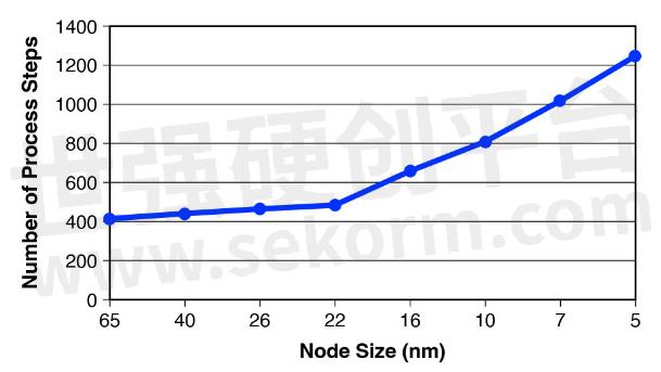
Smaller circuit features have dramatically increased the need for inspection, which is often best performed with lasers.
But a key concept to understand here is that it requires shorter wavelength lasers to push the boundaries of defect detection. This is because the efficiency of light scattering depends on the relationship between the wavelength of the light and the size of the features or defects being inspected. When the feature size is much smaller than the wavelength of the light, scattering becomes less efficient, and the signal from these features or defects diminishes. This means the defects can’t be detected – at least not on timescales relevant for high-volume semiconductor manufacturing.
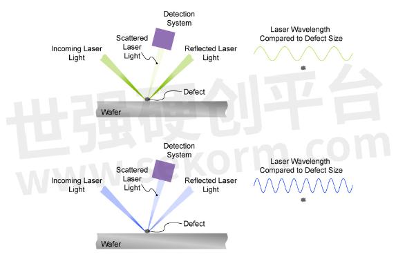
Shorter laser wavelengths are required to detect smaller defects because of the relationship between light scattering and defect size. Currently, 266 nm lasers are used for the most demanding wafer inspection tasks.
Two decades ago, when transistors were a comfortable 110 nm or larger, visible green lasers (532 nm) and ultraviolet (UV) lasers sufficed for defect detection. But shrinking circuit features have propelled the industry towards deep-ultraviolet (DUV) lasers.
Coherent met this challenge head-on with the introduction of our groundbreaking Azure laser in 2002. This laser utilizes Optically Pumped Semiconductor (OPS) technology to produce green output which is then frequency doubled into the DUV (266 nm).
The Azure delivers continuous wave (CW) output at a single, frequency-stabilized wavelength. Its combination of a narrow wavelength, high power, low noise, and extreme stability enables reliable detection of small defects at the speeds necessary for high-throughput semiconductor fabrication.
Coherent distinguishes itself with our ability to make high-power, deep UV lasers that offer exceptional lifetime and reliability. There are several reasons why we’re able to accomplish this.
First, we make our own non-linear crystals. Working in the deep UV demands extraordinarily high-quality crystals manufactured with tremendous precision. The only way we can obtain the quality level we need for our frequency doubling crystals is to make them ourselves.
Next, we employ our own patented PermAlign construction for the optical mounts within the laser itself. These mounts deliver exceptional long-term stability, which means that no adjustments will ever be required. PermAlign mounts allow us to hermetically seal the laser resonator. And this is key to preventing the ingress of any environmental contaminants which might impact laser performance. Plus, the lasers are originally assembled in cleanroom conditions using semi-automated methods to avoid any contamination at the outset. This also ensures a high degree of unit-to-unit consistency.
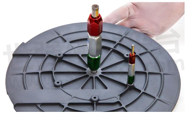
Go/No Go check for part conformance on an in-process wafer chuck.
Another requirement for wafer inspection is high speed motion and part handling mechanics, together with an extremely stable surface (to minimize measurement noise). We supply reaction bonded SiC (RBSiC) for stages and other tooling that deliver the unique mix of low thermal expansion (CTE), high strength, and high strength-to-weight ratio needed for the most demanding inspection systems.
Future Roadmap
As the semiconductor industry progresses towards even smaller nodes, the demands on inspection lasers become even more stringent. Fortunately, this aligns perfectly with our core strengths at Coherent. We maintain close collaboration with leading wafer fab equipment manufacturers, ensuring that our products not only meet, but anticipate, the needs of semiconductor manufacturing processes. Thus, Coherent empowers manufacturers to surmount the inspection challenges of today and tomorrow.
- |
- +1 赞 0
- 收藏
- 评论 0
本文由雪飘梦飞转载自COHERENT Official Website,原文标题为:POWERING ADVANCED SEMICONDUCTOR INSPECTION,本站所有转载文章系出于传递更多信息之目的,且明确注明来源,不希望被转载的媒体或个人可与我们联系,我们将立即进行删除处理。
相关推荐
Caltech: Unlocking Quantum Mysteries
Dr. David Hsieh‘s research at Caltech utilizes the Coherent Astrella laser to study quantum materials, particularly strongly correlated electron systems like Mott insulators. His work has led to the discovery of Hubbard excitons, contributing significantly to quantum mechanics and the understanding of exotic quantum phenomena. The laser‘s precision and reliability have been crucial for these groundbreaking experiments.
Coherent LASER FRAMEWORK助力西门子在其数字工厂中生成标记
借助 Coherent 应用程序开发支持和 Coherent 出品的 Laser FrameWork 软件,西门子能够成功实施其 ID Link 制造计划。
Ytterbium Fiber Lasers Enable Cutting-Edge Neuroscience
The latest generation of ytterbium-based lasers now provides full independent control of both the tunable beam and the fixed wavelength beam, before they leave the laser head, i.e., with guaranteed pulse width and TEM00 beam quality (M2 < 1.1).
电力线F 10/30 QS激光打标机,带绿色光纤激光器
描述- 该资料介绍了两款绿色光纤激光标记机——PowerLine F 10 QS 和 PowerLine F 30 QS。这两款设备适用于半导体IC和其他热敏感元件的浅刻标记,采用绿色波长和纳秒脉冲长度的光纤激光器与高质量扫描光学系统相结合。PowerLine F 30 QS 可作为双头激光标记机使用,以提高效率。软件支持复杂图案设计和变量数据(条形码、序列号)的使用。
型号- F 10 QS,F 30 QS D,F 30 QS
Coherent Announced Latest Generation Adjustable Ring Mode Fiber Laser ARM FL, Reducing the Volume and Footprint by 50%
Coherent announced the launch of its latest generation adjustable ring mode fiber laser ARM FL. This next generation platform, featuring a new advanced controller, offers all the functions of its predecessor while reducing the volume and footprint by 50%.
Coherent Introduces New Laser Welding Head With Tactile Seam-Tracking Technology for Electric Vehicle Manufacturing
Coherent Corp., a leader in advanced laser processing solutions, today introduced HIGHtactile, a new laser welding head with tactile seam-tracking technology ideal for electric vehicle (EV) manufacturing applications.
即插即用的OBIS LX/LS激光器CW固态激光器
描述- Coherent OBIS系列激光器提供高信噪比激光技术,适用于生命科学、环境监测和检测等多个领域。该系列产品基于光泵半导体激光(OPSL)技术和激光二极管解决方案,具有出色的可靠性和性能。OBIS家族覆盖从紫外到近红外波段的波长范围,具备即插即用灵活性,可快速集成并降低时间成本。
型号- OBIS FAMILY,OBIS 473LX,OBIS 413LX,OBIS 514LX,OBIS 685LX,OBIS 640LX,OBIS 660LX,OBIS 637LX,OBIS 375LX,OBIS LX,OBIS 505LS,OBIS 522LX,OBIS 980LX,OBIS,OBIS 808LX,OBIS 405LX,OBIS 561LS,OBIS LS,OBIS 730LX,OBIS 750LX,OBIS 488LS,OBIS 422LX,OBIS 505LX,OBIS 488LX,OBIS 445LX,OBIS 633LX,OBIS 690LX,OBIS 647LX,OBIS 785LX,OBIS 458LX,OBIS 514LS,OBIS 552LS,OBIS 594LS,OBIS 532LS
Coherent Unveils Discovery LX Laser, Provides Ultrashort 100fs Pulses, Expanding the Chameleon Discovery Family
Coherent announces the launch of the Chameleon Discovery LX, the latest addition to the successful Chameleon Discovery product line. Designed for researchers in nonlinear microscopy and ultrafast spectroscopy, this advanced femtosecond laser delivers exceptional performance and versatility to meet evolving market needs.
Coherent Introduced 2x1000mW Dual-Chip Pump Laser Module for Optical Amplification in Optical Networks
Coherent, a leader in pump laser technology for erbium-doped fiber amplifiers (EDFAs) deployed in optical networks, today announced the industry’s first dual-chip pump laser module with up to 1000mW of output power per fiber in a 10-pin butterfly package.
Coherent Introduces New HIGHmotion 2D Laser Processing Head Optimized for Deep Copper Welds Over Wide Working Areas in EV Applications
Coherent, a leader in advanced laser processing solutions, today introduced its new HIGHmotion 2D laser processing head that is rated for 8 kW beam delivery and which has been optimized for deep copper welds over wide working areas in electric vehicle (EV) manufacturing applications.
Coherent Introduces ARM FL20D Fiber Laser, Setting New Standards for High-Power Welding
Coherent today announced the launch of the ARM FL20D fiber laser. This new offering in the highly successful ARM laser family features a new higher power level of 20 kW and a unique dual ring beam configuration.
Coherent Introduces Industry-first Pump Laser Diode with Record 65W Power
Coherent Corp, a leader in high-power semiconductor lasers, announced the introduction of its next-generation pump laser diode, with 65W of output power for fiber lasers in industrial and consumer applications.
Coherent Announces the World’s First 6-inch InP Scalable Wafer Fabs Paving the Way for the Next Generation of Lasers
Coherent expands capacity in its U.S. and European fabs and significantly reduces die cost for InP optoelectronic devices including lasers, detectors, and electronics.
Rapid LX激光系统安装前指南
描述- 本指南为Coherent公司Rapid LX皮秒工业激光系统用户提供安装前准备指导。内容包括系统位置、连接和启动要求,以及安全注意事项。指南详细说明了环境条件、空间和电源需求、OEM要求、交付范围、安装所需工具、冷却器空间要求、电源连接、激光头机械尺寸和连接器功能。此外,还强调了激光安全要求,包括佩戴激光安全眼镜、实施互锁链和紧急停止按钮等。
型号- RAPID LX
电子商城
现货市场
服务
可定制UV胶的粘度范围:150~25000cps,粘接材料:金属,塑料PCB,玻璃,陶瓷等;固化方式:UV固化;双固化,产品通过ISO9001:2008及ISO14000等认证。
最小起订量: 1支 提交需求>
可定制导热胶的导热系数1~6W、粘度范围3000~250000cps、固化方式可加热、仅室温、可UV;施胶方式:点胶机、手工、喷胶、转印;支持颜色、硬度、固化时间等参数的个性化定制。
最小起订量: 1支 提交需求>






登录 | 立即注册
提交评论