Innoscience’s BiGaN technology leads the way toward breakthrough GaN applications for smartphones




The UFCS Technical Seminar of the 1st Plug Conference of Guangdong Terminal Fast Charging Industry Association was successfully held on June 28. At the seminar, the Association's Technical Committee and Technical Research Working Group made a detailed introduction to the development trend of fast charging technologies, critical points of UFCS technical standards, and cutting-edge achievements of UFCS technologies.
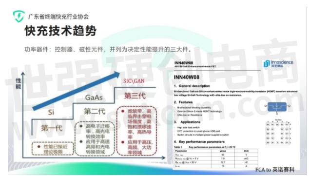
The plug conference has accelerated the standardization and widespread application of terminal fast charging technologies by bringing together players in the fast charging industry who join hands to promote the research of relevant application scenarios, requirements, technologies, and standards in the fast charging industry.
In the plug conference, the father of OPPO VOOC Flash Charge unveiled Innoscience's(英诺赛科) Bi-GaN series for the first time, and the INN40W08 GaN switching tube of the Bi-GaN series also made its appearance.
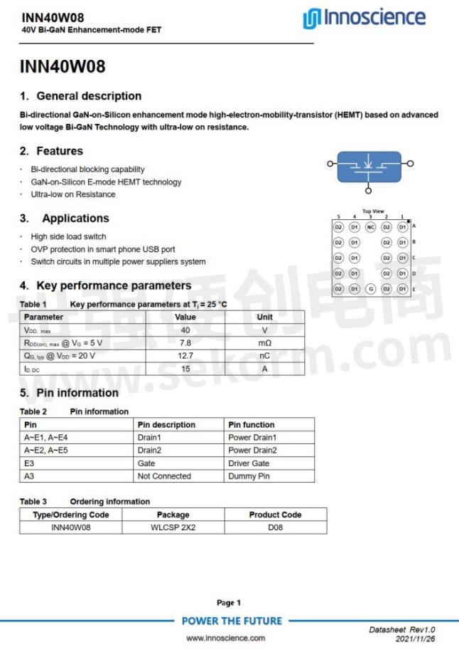
Innoscience INN40W08 is a 40V enhanced small-sized switching tube in the Bi-GaN product family that is packed in a WLCSP 2x2 package. The chip supports bidirectional switching with on-state resistance as low as 7.8mΩ. It can be used in scenarios such as overvoltage protection circuits for smartphone charging, high-side load switching circuits, and switching circuits for multi-power systems.
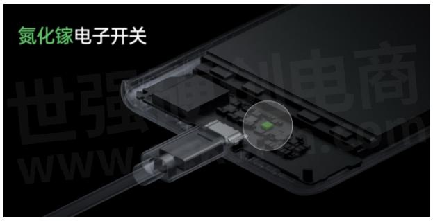
It is learned that OPPO has already adopted GaN switching tubes in its models with mass production, making it the world's first cell phone manufacturer with built-in GaN charging protection. The technology will also be applied in large quantities in OPPO's future models, which will be a significant move in the industry.
For a long time, silicon MOSFETs have been used in cell phones’ internal power switching devices. However, they not only occupy much space on the motherboard of cell phones but also lead to considerable temperature rise and power loss in case of high power fast charging, which affects the stability and high power duration of fast charging.
As a third-generation semiconductor material, GaN has superior characteristics such as high frequency, high efficiency, and low resistance, which are vital for efficient charging. In the past, the charging protection was built into the phone charger through GaN power devices. However, with Bi-GaN, GaN chips are now built into the phone.
Thanks to GaN's small resistance per unit length and the fact that it does not have parasitic diodes, one Bi-GaN can be used to replace the previous connected back-to-back NMOS in a common-drain configuration to realize bidirectional switching of a battery's charging and discharging currents, reducing on-state resistance by 50% and temperature rise by 40% in the same board area.
As the charging power of cell phones continues to increase, Innoscience's Bi-GaN series products not only save valuable space inside the phone but also reduce the temperature rise of the phone during charging, maintain a more comfortable temperature during fast charging, extend the duration of fast charging, and provide a better charging experience for users.
It is learned that Innoscience will soon release INN040W048A, the next generation of its BiGaN series, with the same size, 50% reduction in Rds on, and minor conduction loss, making it more competitive in higher power fast charging scenarios. So let's wait and see.
With years of experience in the field of GaN, Innoscience has become the world's leading chip manufacturer and has made breakthroughs in the core technology and critical process of 8-inch GaN-on-Si. Innoscience delivers solutions with internationally advanced performance and has worked with multiple top brands in product and solution design, which customers widely recognize. The application of its Bi-GaN products in the internal power switch of smartphones also marks the arrival of a new era of GaN application.
So far, the application of GaN in the fast charging of consumer goods has been moved to the fast track. In the near future, with its high power density, high frequency, and efficiency features, the application scope of GaN will gradually expand to more fields including new energy vehicles, solar energy, data center, artificial intelligence, and 5G communications, thus becoming an essential part of our everyday life.
- |
- +1 赞 0
- 收藏
- 评论 0
本文由董慧转载自英诺赛科,原文标题为:Innoscience’s BiGaN technology leads the way toward breakthrough GaN applications for smartphones,本站所有转载文章系出于传递更多信息之目的,且明确注明来源,不希望被转载的媒体或个人可与我们联系,我们将立即进行删除处理。
相关推荐
英诺赛科多款TO252/TO220封装的GaN强势出货,耐压从650V升级到700V为电源设计提供丰富选择
英诺赛科推出多款采用TO252/TO220 封装的直驱氮化镓芯片INN700TK140C、INN700TK190B、INN700TH240B,基于先进的8英寸硅基氮化镓技术,耐压从650V升级到700V,并迅速量产出货,为终端产品的电源设计提供了丰富选择。
原厂动态 发布时间 : 2023-08-08
英诺赛科荣获“2023年行家说极光奖”三大奖项,未来将持续推进氮化镓的深入应用
12月13-14日,由行家说主办的第三代半导体年会(碳化硅&氮化镓产业发展高峰论坛暨行家说极光奖颁奖典礼)在深圳成功举办。在2023行家极光奖颁奖典礼上,英诺赛科荣获“第三代半导体年度中国领军企业”、“中国GaN十强企业”和“年度最具影响力产品”三大奖项。
原厂动态 发布时间 : 2023-12-19
英诺赛科连续两年荣获全球最具潜力第三代半导体技术奖,LLC-DCXIBC模块助力数据中心系统效率全面提升
英诺赛科受邀参与IIC高效电源管理及宽禁带半导体技术应用论坛,并被评选为2023年全球电子成就奖-最具潜力第三代半导体技术企业,其InnoGaN助力高频高效高功率密度电源发展,提升数据中心效率。
原厂动态 发布时间 : 2023-11-14
英诺赛科(Innoscience)高压GaN FET/低压GaN FET/晶圆选型表
描述- 英诺赛科成立于2015年12月,是一家致力于第三代半导体硅基氮化镓研发与产业化的高新技术企业。公司采用IDM全产业链模式,集芯片设计、外延生长、芯片制造、测试与失效分析于一体,拥有全球最大的8英寸硅基氮化镓晶圆的生产能力。主要产品涵盖从低压到高压(30V-650V)的氮化镓功率器件,产品设计及性能均达到国际先进水平。
型号- INN150LA070A,INN650DA04,INN650D260A,INN650D150A,INN100W08,INN040LA015A,INN100W14,INN650D190A,INN650D080B,INN40W08,INN650N500A,INN650D350A,INN040W048A,INN650TA030A,INN650DA190A,INN650DA350A,INN650N260A,INN650DA150A,INN650DA260A,INN100W032A,INN650N150A,INN650TA080A,INN650N140A,INN650N240A
Innoscience Delivers 40V Bi-directional GaN HEMT with Ultra-low on Resistance of 7.8mΩ for Mobile Devices, Chargers and Adapters
Innoscience announced the INN40W08, a 40V bi-directional GaN-on-Si enhancement mode high-electron-mobility-transistor (HEMT) for mobile devices. The INN40W08 HEMT has been developed using the company‘s advanced InnoGaN technology which features ultra-low on resistance.
新产品 发布时间 : 2023-04-11
【应用】OPPO VOOC闪充之父首次展示了英诺赛科Bi-GaN系列增强型开关管,实现智能手机氮化镓应用新突破
在氮化镓领域深耕多年的英诺赛科,拥有全球领先的芯片制造能力,在8英寸硅基氮化镓核心技术和关键工艺领域实现了重大突破,产品性能已达到国际先进水平。其Bi-GaN产品在智能手机内部电源开关领域的落地,也标志着氮化镓应用的全新时代已经到来。
应用方案 发布时间 : 2022-08-02
【应用】英诺赛科氮化镓开关管助力双向AC-DC变换器设计,转换效率达95%
芯仙能源技术推出的这款双向AC-DC变换器具备2000W输出功率,支持整流输出模式和逆变模式,适合用于48V电池系统的储能应用等场合。逆变模块内部采用英诺赛科的氮化镓器件、继电器来自Churod中汇瑞德,线圈电压12V,触点容量50A;通过纳芯微驱动器驱动氮化镓开关管,交流输入和输出保险丝来自华德电子,为WM50系列电力熔断器。
应用方案 发布时间 : 2023-03-04
【应用】iQOO手机原装120W超快迷你充电器,内置英诺赛科定制氮化镓芯片,支持超高开关频率
充电头网最近拿到了iQOO手机标配的一款120W超快闪充迷你充电器,这款充电器内置英诺赛科定制氮化镓功率芯片,由奥海科技代工生产,整体十分小巧且通用性不错。 充电器不仅支持自家私有闪充,还支持65W PD快充以及具备PPS电压档位,可以满足绿厂用户外出情况下,手机和笔记本电脑共用充电,降低携带成本。
应用方案 发布时间 : 2023-04-26
【应用】英诺赛科60W氮化镓LED驱动电源方案,支持90~264V输入电压,满载输出效率达93.5%
英诺赛科推出了一款60W LED驱动电源参考设计,这款电源为单级高PF值反激设计,并且为原边反馈,无需光耦和输出电流检测电路,在初级完成恒压控制,电路精简,简化设计并降低成本;电源支持90~264V输入电压,220V输入满载输出效率高达93.5%。
应用方案 发布时间 : 2023-03-23
英诺赛科(Innoscience)——世界领先的8英寸硅基氮化镓产业化平台
英诺赛科(Innoscience)创办于2015年12月,是第三代半导体电力电子器件研发与生产的高科技企业。英诺赛科(Innoscience)主要致力于第三代半导体硅基氮化镓功率与射频器件的研发与产业化,并已于2017年底建成了我国首条8英寸硅基氮化镓功率器件的量产线。
品牌简介 发布时间 : 2019-01-16
英诺赛科(Innoscience)INN650D02—650V GaN增强型功率晶体管数据手册
描述- INN650D02 650V GaN Enhancement-mode Power Transistor Datasheet
型号- INN650D02
【应用】漏极电压650V的GaN FET INN650TA030AH用于光伏逆变器,导通内阻30mΩ
随着制作工艺要求越来越高,功率管的选择也要求着更高的耐压,更高的开关频率。针对光伏逆变器的应用设计,本文推荐英诺赛科推出的GaN FET INN650TA030AH,漏极电压可达650V,最大漏源电流100A,导通内阻30mΩ。
应用方案 发布时间 : 2023-02-17
【应用】国产氮化镓场效应晶体管INN650D02实现高效率小型化的65W A+C快充设计
65W的A+C快充设计中快充主要用于反激拓扑电路,控制主回路的开关实现变压器的能量转换。INN650D02是英诺赛科的650V/200mΩ/11A的氮化镓场效应晶体管,采用该氮化镓场效应晶体管在频率120Khz的情况下可实现高效92.3%的小型化65W A+C快充设计。
应用方案 发布时间 : 2020-09-02
【应用】英诺赛科耐压650V的GaN芯片INN650DA260A助力Realme闪充,有效节省空间
英诺赛科INN650DA260A,耐压650V,瞬态耐压750V,支持超高开关频率,无反向恢复电荷,具有极低的栅极电荷和输出电荷,符合JEDEC标准的工业应用要求。得益于工业的迭代,性能明显提升,适用于65-120W的反激架构,120-200W的LLC架构。
应用方案 发布时间 : 2023-04-29
英诺赛科搭载100V双向导通VGaN的BMS方案,实现充放电控制与保护,大幅减少PCB占板面积
针对BMS应用领域,英诺赛科开发了48V/120A BMS评估板(INNDBMS120LS1),采用新品100V双向导通芯片VGaN INV100FQ030A实现充放电控制与保护,大幅减少PCB占板面积,降低系统成本。
应用方案 发布时间 : 2023-11-04
现货市场
服务
可烧录IC封装SOP/MSOP/SSOP/TSOP/TSSOP/PLCC/QFP/QFN/MLP/MLF/BGA/CSP/SOT/DFN;IC包装Tray/Tube/Tape;IC厂商不限,交期1-3天。支持IC测试(FT/SLT),管装、托盘装、卷带装包装转换,IC打印标记加工。
最小起订量: 1pcs 提交需求>
满足150W内适配器、PD快充、氮化镓快充等主流产品测试需要;并可查看被测开关电源支持协议,诱导多种充电协议输出,结合电子负载和示波器进行高精度测试。测试浪涌电流最大40A。支持到场/视频直播测试,资深专家全程指导。
实验室地址: 深圳 提交需求>








登录 | 立即注册
提交评论