KYOCERA Develops New GaN Laser Chip, World‘s Smallest* to be Mass-Produced from Silicon Working Substrate




KYOCERA Corporation (President: Hideo Tanimoto) has developed a new thin-film process technology for making unique silicon (Si) substrates for gallium nitride (GaN)-based micro-light sources, including short-cavity lasers and micro-LEDs.
*World's Smallest: Among GaN-based edge-emitting lasers formed on silicon substrates. (Source: Kyocera, September 2022)

■ What is a micro-light source?
A "Micro-light source" is a light source with a side measuring less than 100 microns (1/10th of a millimeter). Examples include short-cavity lasers and micro-LEDs. Because they offer key performance advantages, such as higher definition, smaller size, and lighter weight, micro-light sources are considered essential to next-generation automotive displays, KYOCERA arable smart glasses, communication equipment, and medical devices. The market for micro-LED chips alone is expected to reach $2.7 billion by 2026, a compounded annual growth rate (CAGR) of about 241%.*
*Source: TrendForce"Micro LED Large-Sized Display Chip Market Estimated to Reach 2.7 Billion US dollars by 2026, Says TrendForce"(August,2022)
■ Technical challenges in making micro-light sources
GaN-based light-source devices, both micro-LED and laser, have typically been fabricated on sapphire and GaN substrates. Conventional processes involve forming a thin GaN device layer for the light source directly onto the sapphire substrate by heating it to a high temperature (1,000 degrees C or more) in a controlled gas atmosphere. The device layer has to be then removed, or "peeled," from the substrate to create a GaN-based micro-light-source device. Despite rising demand for smaller devices, however, three separate challenges threaten the ability of this process to achieve miniaturization targets in the near future:
① Difficulty in peeling the device layer
In case of micro-LEDs, current processes require difficult steps to divide the device layer into individual light sources on the substrate; and then, to separate (or "peel") the device layer from the substrate. As devices become smaller, the technical challenge of this peeling process can result in unacceptably low yield.
② High defect density, inconsistent quality
Fabrication of micro-light sources is also problematic because device layers must be deposited onto sapphire, silicon, or other materials with crystal structures that differ from that of the device layer. This creates high defect density and inherent quality control challenges.
③ High manufacturing costs
GaN and sapphire substrates are very expensive materials. Although silicon substrates cost less than sapphire, separating the device layer from a silicon substrate is extremely difficult.
■ New process developed by Kyocera
Kyocera successfully developed the new process technology at the company's Research Institute for Advanced Materials and Devices in Kyoto, Japan. First, KYOCERA grows a GaN layer on Si substrate which is available in high volumes at a low cost. The GaN layer is then masked with a non-growing material that features an opening in the center. After this, when a GaN layer is formed on the Si substrate, GaN nuclei grow over the opening in the mask. The GaN layer, which is a growing nucleus, has many defects at the initial stage of growth; but, by forming the GaN layer laterally, high-quality GaN layers with low defect density can be created, and devices can be fabricated successfully from this low-defect region of the GaN layer.
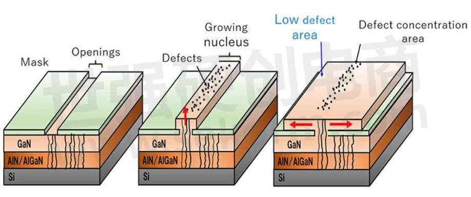
■Advantages of Kyocera's new process (GaN Laser Chip)
① Easier peeling of the GaN device layer
Masking the GaN layer with a material that does not grow suppresses bonding between the Si substrate and the GaN layer, greatly simplifying the peeling process.
② High-quality GaN device layers with low defect density
Since Kyocera's process can deposit low-defect GaN over a wider area than before, consistent fabrication of high-quality device layers is possible.
③ Lower manufacturing costs
Kyocera's new method facilitates successful and reliable separation of the GaN device layer from the relatively inexpensive Si substrate, which will greatly reduce manufacturing costs.
■ Micro-light source applications
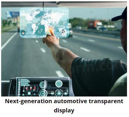
① Next-generation automotive transparent display
In the future, the advent of autonomous driving will create demand for displays that are brighter, higher-definition, power-efficient, more highly transparent, and lower cost.
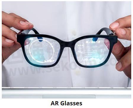
② Micro-light sources for AR/VR
The market for micro-light sources used in augmented reality (AR) and virtual reality (VR) is expected to expand rapidly. Smart glasses and other products are being developed to facilitate the creation of virtual spaces through the metaverse in VR and "de-smartphoning" in AR. While conventional semiconductor lasers for AR have been miniaturized to as small as 300 microns in length, Kyocera is the first in the world to achieve a size of just 100 microns. KYOCERA could achieve this size by developing a completely new production process that is an evolution of cleaving method.
This so-called "novel cleaving method" results in a size reduction of about 67% and helps minimize power consumption. Semiconductor lasers with lower power consumption make it possible to reduce the size and weight of the battery, thus improving fit.
Kyocera will offer a wide range of platform, substrate, and process technologies to bring high-quality, low-cost micro-light sources to market in the near future. KYOCERA also aims to transform next-generation display and laser markets using this new platform.
- |
- +1 赞 0
- 收藏
- 评论 0
本文由Devor转载自KYOCERA News,原文标题为:KYOCERA Develops New GaN Laser Chip, World's Smallest* to be Mass-Produced from Silicon Working Substrate,本站所有转载文章系出于传递更多信息之目的,且明确注明来源,不希望被转载的媒体或个人可与我们联系,我们将立即进行删除处理。
相关推荐
Kyocera Named to “Top 100“ Global Innovators List for Third Consecutive Year, Marking Eighth Appearance
Kyocera Corporation announced that it has been recognized as a Top 100 Global Innovators™ 2024 by Clarivate™, a leading global provider of transformative intelligence. This year‘s list brings Kyocera‘s eighth appearance, with 2024 marking the third consecutive year.
KYOCERA Lanuched Ultra-Small Crystal Units CX1008SB Series Achieving the Same Performance as Kyocera‘s Previous With A 33% Reduction in Size
Kyocera‘s new generation of ultra-small crystal units (CX1008SB series) components - WINNER of the Japan Ministry of Education, Culture, Sports, Science and Technology (MEXT) award for technology development in 2021 for achieving the same performance as our previous crystal units with a 33% reduction in size.
KYOCERA Named Among “Top 100“ Global Innovators for 7th Year by Clarivate
Kyocera has been recognized as a Top 100 Global InnovatorTM 2023 by Clarivate, a global leader in connecting people and organizations to intelligence that transforms the world. This year marks Kyocera Corporation‘s seventh appearance on the list, including consecutive listings in 2022 and 2023.
Kyocera(京瓷)工业TFT LCD显示屏选型指南
目录- TFT LCDs introduction TFT LCD,Value-Line TFT LCD LCD ToolKIT
型号- TVL-55731GD032J-LW-G-AAN,T-55548GD057JU-LW-ABN,T-55788GD121J-LW-AAN,T-55787GD104J-LW-ACN,TCG062HVLDA-G20,TCG057QVLGA-G00,TCG075VGLCE-G00,T-55149GD030J-MLW-AQN,TCG070WLPAANN-AN00,TCG084SVLQAPNN-AN20,T-51750GD065J-LW-AON,TCG075VGLDA-G00,TVL-55739GD032J-LW-G-AAN,TCG057QVLBA-G00,T-55619GD065J-LW-AAN,TCG057VGLCA-G00,TCG104SVLPAANN-AN20,TCG121SVLPAANN-AN*16,TCG121SVLQAPNN-AN20,TVL-55730GD035JU-LW-G-ABN,TVL-55789D133-LW-I-AAN,T-55786GD084J-LW-ACN,TCG084SVLP*ANN-AN*13,TVL-55724GD043J-LW-G-AAN,TVL-55684D140U-LW-I-AAN,T-55343GD035JU-LW-ADN,TCG121WXLP*PNN-AN*01,TVL-55737GD030J-LW-G-AAN,TVL-55729D090J-LW-I-AAN,TCG057QVLCA-G00,TCG057VGLCS-H50,T-55620GD057JU-LW-AAN,T-55520GD057J-LW-ACN,TCG085WVLQDPNN-GN00,TCG104VGLAAANN-AN20,T-55788GD121J-LW-ACN,TCG057QVLCS-H50,TCG070WVLPEANN-AN20,TCG084SVLPAANN-AN20,TVL-55682D101U-LW-I-AAN,TCG070WVLQAPNN-AN00,TCG075VGLEAANN-GN00,T-55787GD104J-LW-AAN,TCG043WQLBAANN-GN00,TVL-55733GD035J-LW-G-AAN,TCG057VGLGA-G00,TCG070WVLPAANN-AN50,TCG101WXLP*ANN-AN*03,TCG035VLPAANN-AN00,TVL-55683D116U-LW-I-AAN,TVL-55736GD032JR-LW-G-AAN,TCG104VGLABANN-AN50,TVL-55728D070J-LW-I-AAN,T-55265GD057J-LW-ADN,TVL-55738GD032J-LW-G-AAN,TCG121XGLP*PNN-AN*37,TCG085WVLCB-G00,TVL-55911D150-LW-I-AAN,TCG084VGLAAANN-AN50,TCG121SVLPAANN-AN20,T-55786GD084J-LW-AAN,TCG121SVLPBANN-AN00,TCG070WVLPEANN-AN30,TCG043WQLBAANN-GN50,T-55785GD070J-LW-ABN,TCG104SVLPEANN-AN30,TCG084VGLAAANN-AN00,TCG104SVLQAPNN-AN20,TVL-55790D133-LW-I-AAN,TCG084VGLACANN-AN00,T-51750GD065J-LW-ANN,TCG070WVLQEPNN-AN20,TVL-55806GD040J-LW-G-AAN,TCG057VGLBA-G00,TCG104VGLAAANN-AN00,TVL-55781GD050J-LW-G-AAN
KYOCERA SAW滤波器选型表
提供平衡型、不平衡型,应用于4G、5G以及基站,多种BAND的SAW滤波器
|
产品型号
|
品类
|
生产状况
|
BAND
|
尺寸(LxW) (mm)
|
类型
|
High Power Durability
|
用途
|
系列
|
厚度(Max.) (mm)
|
工作温度范围(Min.) (℃)
|
工作温度范围(Max.) (℃)
|
包装形式
|
参照型号
|
RoHS指令对应状況
|
|
SF20-2595M3UUA1
|
SAW滤波器
|
量产品
|
41TRx
|
2.0mmx1.6mm
|
Unbalanced Type
|
|
基站
|
SF20
|
0.90mm
|
-40℃
|
95℃
|
Reel
|
|
RoHS指令
|
选型表 - KYOCERA 立即选型
Kyocera Introduces Cutting-Edge Peltier Module with 21% Increase in Cooling Performance
Kyocera Corporation (President: Hideo Tanimoto, hereinafter: Kyocera) today introduced a new Peltier (thermoelectric) module with improved heat absorption. This new Peltier module has a maximum heat absorption rate*1 21% higher than Kyocera‘s conventional products, enabling dramatically enhanced cooling performance.
KYOCERA 板对板连接器选型表
可用于芯间距0.35mm~2.54mm,芯数1~180,嵌合高度0.6mm~30mm,宽度1.7mm~12.4mm,采用DIP、SMT基板安装方式
|
产品型号
|
品类
|
生产状况
|
芯间距(mm)
|
连接方式
|
嵌合高度 (mm)
|
宽度(mm)
|
芯数
|
浮动 (mm)
|
工作温度范围(Min.) (℃)
|
工作温度范围(Max.) (℃)
|
高速传输
|
系列
|
形状
|
额定电流(信号)(A)
|
额定电流(电源)(A)
|
额定电压 (V)
|
耐压值 (Vrms)
|
金具
|
Boss
|
Vacuum item
|
RoHS指令对应状況
|
包装形式
|
|
148152030035868+
|
板对板连接器
|
量产品
|
0.400mm
|
基板平行插接
|
3.50mm
|
4.30mm
|
30
|
XY±0.4mm
|
-40℃
|
105℃
|
MIPI D-PHY,PCI Express Gen2 & 3
|
8152
|
Plug
|
DC 0.3A/Contact
|
|
DC 30V/Contact
|
AC 250Vrms、1min.
|
金具
|
Without
|
Without
|
RoHS指令
|
Reel
|
选型表 - KYOCERA 立即选型
KYOCERA FPC/FFC连接器选型表
可用于芯间距0.2mm~1mm,芯数3~100,板上高度0.9mm~6mm,宽度2.7mm~8.6mm
|
产品型号
|
品类
|
生产状况
|
芯间距(mm)
|
连接方式
|
板上高度 (mm)
|
宽度(mm)
|
芯数
|
锁扣方式
|
接点位置
|
工作温度范围(Min.) (℃)
|
工作温度范围(Max.) (℃)
|
高速传输
|
适合FPC/FFC高度(mm)
|
系列
|
额定电流(信号)(A)
|
额定电压 (V)
|
耐压值 (Vrms)
|
备注
|
RoHS指令对应状況
|
包装形式
|
参照型号
|
|
046251033010846+
|
FPC/FFC连接器
|
计划中
|
0.500mm
|
垂直嵌合
|
5.45mm
|
3.50mm
|
33
|
Flip lock
|
单面接点
|
-40℃
|
105℃
|
|
0.3mm
|
6251
|
DC 0.4A
|
DC 50V
|
AC 200Vrms、1min.
|
|
RoHS指令
|
Reel
|
|
选型表 - KYOCERA 立即选型
Kyocera Launches New Cut-off Solution “KGZ“ for Small Parts machining
A newly developed unique clamp structure and new insert shape realize high efficiency and stable machining. New specialized PVD coating released at the same time.Kyoto, 20th June 2024. Kyocera Corporation announced that it has developed a new cut-off solution, “KGZ“, for small parts machining.
KYOCERA 时钟晶体振荡器选型表
提供了2016封装到7050封装的时钟振荡器(SPXO)选型,可对应多种频率,电源电压可用于1.8V/2.5V/3.3V、2.5V/3.3V、2.5V以及3.3V
|
产品型号
|
品类
|
生产状况
|
类型
|
尺寸(LxW) (mm)
|
厚度(Max.) (mm)
|
频率(MHz)
|
工作温度范围(Min.) (℃)
|
工作温度范围(Max.) (℃)
|
频率容差(x10⁻⁶)
|
输出类型
|
电源电压(V)
|
AEC-Q
|
用途
|
INH功能
|
系列
|
质量
|
包装形式
|
RoHS指令对应状況
|
|
KC2016K1.50000C10E00
|
时钟振荡器
|
量产品
|
Standard type
|
2.0mm×1.6mm
|
0.80mm
|
1.5MHz
|
-10℃
|
70℃
|
±50
|
CMOS
|
1.8V,2.5V,3.3V
|
|
Consumer/Industrial/Network/Base station
|
INH功能
|
KC2016K
|
7.01
|
Reel
|
RoHS指令
|
选型表 - KYOCERA 立即选型
KYOCERA SAW双工器选型表
提供分离发送信号(Tx)和接收信号(Rx)的器件,由两个带通滤波器组成,采用平衡型、不平衡型,尺寸含1.6mmx1.2mm、1.8mmx1.4mm、2.5mmx2mm
|
产品型号
|
品类
|
生产状况
|
BAND
|
尺寸(LxW) (mm)
|
类型
|
High Power Durability
|
用途
|
系列
|
厚度(Max.) (mm)
|
工作温度范围(Min.) (℃)
|
工作温度范围(Max.) (℃)
|
包装形式
|
参照型号
|
RoHS指令对应状況
|
|
SD16-0782R8UUA1
|
SAW双工器
|
量产品
|
13
|
1.6mmx1.2mm
|
不平衡型
|
for 5G
|
for Mobile
|
SD16
|
0.65mm
|
-30℃
|
85℃
|
Reel
|
|
RoHS指令
|
选型表 - KYOCERA 立即选型
KYOCERA 陶瓷电容器参数对照表
可用于厚度0.22mm~2.7mm,采用薄层化与高精度技术,工作温度从最低-55℃到最高125℃
|
产品型号
|
品类
|
旧型号
|
生产状况
|
系列
|
尺寸(L) (mm)
|
尺寸(W) (mm)
|
尺寸(T) (mm)
|
温度特性
|
工作温度范围(Min.) (℃)
|
工作温度范围(Max.) (℃)
|
温度特性变化率
|
静电容值
|
静电电容值允差
|
Tanδ
|
Q值
|
包装形式 (Reel dia./pitch)
|
质量(mg)
|
标准/个别
|
RoHS指令对应状況
|
|
KAM05AR70J105KH
|
陶瓷电容器
|
AR05X7R105K06AH
|
量产品
|
KAM
|
1.0mm±0.05mm
|
0.5mm±0.05mm
|
0.5mm±0.05mm
|
X7R(EIA)
|
-55℃
|
125℃
|
±15%
|
1uF(105)
|
K(±10%)
|
7.5
|
|
φ180/2mm
|
1.640mg
|
标准规范
|
RoHS指令
|
选型表 - KYOCERA 立即选型
KYOCERA 电线对电线/电路板连接器选型表
可用于芯间距0.9mm~6.35mm,芯数0~130,嵌合高度0.9mm~3.61mm,采用DIP、SMT基板安装方式
|
产品型号
|
品类
|
生产状况
|
类型
|
电线
|
形状
|
基板安装方式
|
芯数
|
工作温度范围(Min.) (℃)
|
工作温度范围(Max.) (℃)
|
系列
|
额定电流(信号)(A)
|
额定电压 (V)
|
耐压值 (Vrms)
|
RoHS指令对应状況
|
包装形式
|
|
149715000000825+T
|
电线对电线/电路板连接器
|
量产品
|
Branch Connectors
|
Copper Wire:0.3 to 0.5sq,Aluminum Wire:0.5 to 0.75sq
|
ASSY
|
|
1
|
-40℃
|
85℃
|
9715
|
AC/DC 7 to 9A
|
AC/DC 125V
|
AC 1000Vrms、1min.
|
RoHS指令
|
Bag
|
选型表 - KYOCERA 立即选型
京瓷AVX 500系列BMC宽带微波电容器S参数测试法
描述- 本资料提供了KYOCERA AVX 500系列宽带微波电容器(BMC)的S参数测试方法。内容包括了用于生成S参数文件的矢量网络分析仪型号、测试配置、校准套件、测试电缆等信息,并说明了电容器的电容范围和频率范围。
型号- KYOCERA AVX 500 SERIES,KYOCERA AVX 500
【选型】Kyocera(京瓷)SKC TFT型号参数快速参考选型指南
目录- SKCTFT显示器 TFT显示器 TFT显示器高亮产品 SKC开发中型号(-S)
型号- TG060AALPAANN-GN20,TCG075VGLCX-G00,TCG062HVLDA-G20,TCG084VGLACANN-AN00-S,TCG084VGLAAANN-AN20,TCG057QVLPBAFB-GA00,TCG057VGLBA-H50,TCG084SVLPAAFA-AA30-S,TCG057VGLBD-G00,TCG075VGLCF-G00,TCG121XGLPAPNN-AN20,GTCG084SVLQAPNN-AN20,TCG057VGLGC-G00-S,TCG084SVLQAPFA-AA20,TCG057VGLCB-G00,TCG085WVLCL-G00,TCG084SVLPAANN-AN30,STCG057QVLAC-G00,TCG121SVLQAPNN-AN20,TCG121SVLPAANN-AN00,TCG035QVLPDANN-AN50,TCG104SVLQ*PFA-AA*53,TCG075VGLEAAFA-GA00-S,TCG057VGLGC-G50-S,TCG057QVLCA-G00,TCG057QVLCA-G01,TCG075VGLDA-G50,TCG057QVLAL-G00,TCG057VGLCAM-C50,TCG057VGLBA-G20,TCG070WVLQ*PNN-AN*180,TCG084SVLPAANN-AN20,TCG121WXLR*VNN-AN*26,STCG057QVLAF-G00,TCG084SVLQ*PNN-AN*32,TCG084SVLQ*PNN-AN*33,TCG070WVLPCANN-GN01,TCG070WVLPEAFA-AA20,TCG084SVLPAAFA-AA20,TCG070WVLQ*PGA-AC*181,TCG104VGLP*ANN-AN*46,TCG084SVLPAANN-AN30-S,TCG070WVLPEAFA-AA30,TCG101WXLPAANN-AN20-S,TCG121WXLR*VNN-AN*19,TCG121WXLR*VNN-AN*18,TCG121WXLR*VNN-AN*35,TCG070WVLPAANN-AN00-S,TCG104VGLA*ANN-AN*24,TCG104VGLAAANN-AN20-S,TCG104XGLPBPNN-AN70,TCG090WVLPBANN-GN00-S,TCG121SVLPAANN-AN20-S,TCG121XGLPAPNN-AN22-S,TCG043WQLBCBFA-GA50,TCG104SVLPAANN-AN20-S,TCG104SVLPBANN-AN20,TCG121XGLPCPNN-AN70,TCG104SVLPEANN-AN30,TCG084VGLAAANN-AN00,TCG062HVLDA-G22,TCG070WVLQEPFB-AA20,TCG057VGLCAJ-G00,TCG084VGLAAANN-AN00-S,TCG085WVLCA-G00,TCG121WXLR*VNN-AN*27,TCG057VGLBA-G00,TCG070WVLPAANN-AN00,TCG084SVLQAPNN-AN20-S,TCG057VGLBB-H50,TCG070WVLS*QP*-AN*202,TCG070WVLPAAFA-AA00,TCG075VGLCE-G00,TCG057QVLGC-G00GP,TCG057QVLPBANN-GN00,TCG104XGLP*PC*-AD*10,TCG075VGLDA-G00,TCG057QVLPEANN-GN00-S,TCG070WVLQ*PNN-AN*154,TCG075VGLDB-G00-S,TCG104XGLP*PC*-AD*17,TCG070WVLPEAFB-AA00,TCG062HVLQ*VNN*-GN*01,TCG043WQLBBANN-GN50,TCG043WQLBAAFA-GA50,TCG057QVLGC-G00,TCG057VGLBB-G20,TCG104SVLPBANN-AN00,STCG057QVLAA-G00-S,TCG121WXLRDVNN-AN70-E1,STCG057QVLAB-G00,TCG084SVLPAANN-AN20-S,TCG057QVLCT-H50,STCG057QVLAD-G00-S,TCG104XGLPAPNN-AN30,TCG057QVLAD-G02,TCG057QVLBA-H50,TCG057QVLAD-G00,STCG057QVLAB-G00-S,TCG057QVLCS-H50,TCG057QVLPEANN-GN00,TCG070WVLPEANN-AN20,TCG070WVLQGPGK-AD70,TCG104SVLQGPNN-AN40,TCG121WXLP*PC*-AD*20,TCG084VGLAAAFA-AA00,TCG043WQLBAANN-GN00,TCG075VGLP*ANN-GN*12,TCG035QVLPCANN-AN00,TCG035QVLPDAFA-GA50-S,TCG057VGLGA-G00,TCG104XGLPAPNN-AN40,TCG057QVLGA-G00GP,TCG035QVLPDANN-GN50-S,TCG075VGLDA-G20,TCG057VGLGA-G00-S,TCG057QVLCE-G00,TCG057QVLPPANN-GN00,TCG084SVLPAAGL-AB20,TCG057VGLBB-G00,TCG121SVLPBANN-AN00,TCG070WVLPEANN-AN30,TCG057VGLBB-G01,TCG121XGLPAPNN-AN20-S,STCG057QVLAG-G00,TCG035QVLPDANN-GN50,TCG084SVLPAAFA-AA20-S,TCG104SVLQAPNN-AN20,TCG085WVLCAANN-GN00,TCG075VGLDA-H50,TCG070WVLPEANN-AN00,STCG057QVLAA-G00,TCG057QVLHA-G50,TCG057VGLGA-G50-YA,TCG121SVLQEPNN-AN20,TCG062HVLQ*VC*-GD*06,TCG075VGLDB-G00,TCG070WVLPEANN-AN00-S,TCG121XGLPBPNN-AN40,TCG104SVLPAAGP-AC20,TCG104SVLQAPFA-AA20,TCG057QVLAJ-G00,TCG057QVLBA-G00,TCG121SVLRAPNN-AN20,TCG085WVLCU-G00,TCG104SVLPAANN-AN20,TCG084VGLAAAFA-AA50,TCG121SVLPAAFA-AA20,TCG057VGLAD-G00,STCG057QVLAM-G02-S,TCG070WVLQ*PF*-AA*162,TCG104SVLPAAGP-AB20,TCG057QVLAC-G01,TCG121SVLPBANN-AN20,TCG057QVLAC-G00,TCG070WVLPAAFA-AA50,TCG104SVLQ*PNN-AN*37,TCG057VGLCS-H50,TCG057VGLCS-H50-S,TCG070WVLQ*PGK-AD*182,TCG104VGLAAANN-AN20,TCG057VGLGC-G00,TCG043WQLBAAFA-GA00,TCG104SVLQAPCA-AD20,TCG057QVLCB-G00,TCG075VGLEAANN-GN00,TCG057QVLCB-G02,TCG057QVLBB-H50,TCG121XGLPBPNN-AN40-S,STCG057QVLAD-G00,TCG075VGLEAAFA-GA00,TCG035QVLPAANN-AN00,TCG057QVLBA-G20,TCG085WVLDT-G00,TCG104XGLPBPNN-AN701,TCG075VGLDB-H50,TCG070WVLPAAFB-AA00,TCG121SVLQ*PNN-AN*47,TCG121WXLPAPNN-AN20,TCG121SVLQ*PNN-AN*48,TCG104XGLPAPFA-AA30,TCG070WVLPCANN-GN01-S,TCG070WVLQEPNN-AN20,TCG075VGLEAANN-GN00-S,TCG062HVLDB-G20,TCG057QVLAK-G00,TCG057QVLBB-H30,TCG070WVLPAANN-AN50-S,TCG104VGLP*ANN-AN*25,TCG057QVLGA-G00,TCG070WVLPCANN-AN00,TCG057QVLCL-G00F,TCG057VGLCT-H50-S,TCG084SVLQAPNN-AN20,TCG104VGLPCANN-AN40,TCG121WXLPAPNN-AN20-S,TCG104SVLPAAFA-AA20-S,TCG057QVLPEANN-GN60,TCG057QVLCP-G00,TCG057VGLCA-G00,TCG121SVLPJANN-AN50,TCG085WVLCF-G00,TCG121SVLPAANN-AN*16,TCG057QVLBB-G20,TCG104VGLAAAFA-AA00,TCG084VGLAAAFA-AA00-S,TCG104XGLPAPNN-AN30-S,TCG070WVLQGPNN-AN40,TCG070WVLQGPNN-AN41,TCG070WVLPCANN-AN00-S,STCG057QVLAG-G00-S,TCG085WVLQDPNN-GN00,TCG035QVLPAAFA-AA00,TCG070WVLQAPNN-AN01,TCG070WVLQAPNN-AN00,TCG062HVLQ*VNN-GN*01,TCG057VGLCT-H51-S,TCG057QVLCC-G00,TCG070WVLPAANN-AN50,TCG070WVLQAPFA-AA00,TCG057QVLAF-G00,TCG057QVLPAAFB-GA00,TCG057QVLCL-G00,TCG104VGLABANN-AN50,TCG104SVLPAANN-AN00,TCG057VGLAAANN-GN20,TCG085WVLCB-G00,TCG057QVLBB-G00,TCG084VGLAAANN-AN50,TCG104VGLAAAFA-AA20,TCG121SVLPAANN-AN20,TCG101WXLPAANN-AN20,TCG104XGLPAPNN-AN31-S,TCG104SVLQ*PNN-AN*55,TCG104SVLQ*PNN-AN*52,TCG057QVLPEAFC-GA60,TCG084VGLACANN-AN00,TCG104SVLPAAFA-AA20,TCG104VGLAAANN-AN00
电子商城
现货市场
服务
可贴片PCB尺寸50*50mm-580*610mm;PCB厚度0.3-8mm;贴装精度CHIP元件+0.03,BGA Pitch 大于0.25mm;元件尺寸0201-74*74BGA;元件高度:30mm。
最小起订量: 1 提交需求>
可定制LAMP LED、 CHIP LED、 PLCC LED、 汽车用车规级LED、COB LED的尺寸/电压/电流等参数,电压1.5-37V,电流5-150mA,波长470-940nm。
最小起订量: 30000 提交需求>




登录 | 立即注册
提交评论