Reducing Noise Issues in Microcontroller Systems - Part 4


In this short series of Reducing Noise Issues in Microcontroller Systems blogs, we have looked at noise and how it can disturb the opeRAtion of microcontroller-based systems and presented some of the "rules" we can use to minimize the impact of noise in our systems.
Due to the popularity of this series of blogs, we have decided to add this blog as a bonus "extra" to look at some of the features of our RA microcontrollers that can help make a system more reliable in the presence of noise.
In any system, the best way to avoid noise problems is to consider noise reduction from the beginning of the design. It’s important to understand the environment that your system will operate in, what noise sources will be present, and what steps you can take to mitigate these.
It’s always worth spending some time to consider these issues at the start of the design, as it’s much easier to design noise mitigations from the start than to add them at the end of the design, or even worse, have to modify your design when you discover noise problems in the field.
However, sometimes it’s not possible to completely remove every source of noise, and RENESAS RA microcontrollers offer a range of features that can help you make your applications more robust.
In any microcontroller we have to take great care of the system's pins, these are pins that are intrinsic to the operation of the device, and include the supply pins (Vss, Vcc, Vcl, etc.), clock pins, the reset pin, any analog reference pins, the debug pins, and the mode pin (used for controlling the operating mode of the device, such as the boot mechanism).
Each of these pins should receive special consideration in the PCB layout to make sure they operate reliably, as noise on these pins could be fatal for your application.
As we’ve already discussed in previous Reducing Noise Issues in Microcontroller Systems blogs, a good PCB layout is critical in reducing noise, and great care needs to be taken in the design of the power supply and ground system, especially as today's MCUs are typically capable of much faster operation than older devices. Carefully consider the circuit layout, and consider ground return paths, especially for high-speed, high-current signals.
One of the first issues I always ask when I hear about noise issues in a design is do you really need to run so fast, sometimes you need your device to run at maximum speed, but often you do not. The maximum speed may be dictated by the baud rate you need for your UART or by the time you have to complete a Fast Fourier Transform (FFT) filter function, however much of the time, and for many designs, we don’t need to run at the full speed the device is capable of.
We would always recommend that you run as slow as you can to achieve everything you need to achieve and not faster; the faster you go, the faster the signals and the more problems you may have. The slower you go, the less current you take, the less current is switching in your power supply, and the less noise is generated. And, sometimes your power supply will be cheaper because of this. For some things, slower is almost always better.
The RA microcontrollers have the capability to "throttle" their speed, you can change the clock dividers dynamically if required to speed up and speed down. This can sometimes add a lot of complexity to an application as you have to manage the peripheral clocks, but it’s always worth considering if you can reduce the clock speed.
And talking of power supplies, always make sure the power supply's dimensions are correct for your design, don’t always try to reuse the same power supply circuit, and make sure it’s capable of supplying the maximum amount of current you require, as if your supply droops occasionally, this can cause noise issues as well as can generate other system problems.
The datasheet of the RA family carefully documents the capability of each of the I/O pins on each of these devices, there is also a very useful application note available on the Renesas website that details the injection current our devices can withstand to prevent damage to the RA MCU.
Typically most of the standard digital I/O pins (5V tolerant pins on 3V devices, or devices supporting I2C or some other special functions that do not have Schmitt trigger input) on the RA microcontrollers have Schmitt trigger inputs, which can help us make sure fast signal level changes do not propagate into the logic of our device. It’s important to consider the current that will be flowing into and out of the pin, both in normal operation, and if noise is present in the system, the use of current limiting resistors on I/O pins can sometimes be advisable to limit these effects, even external filtering or a protection circuit may be required in extreme cases.
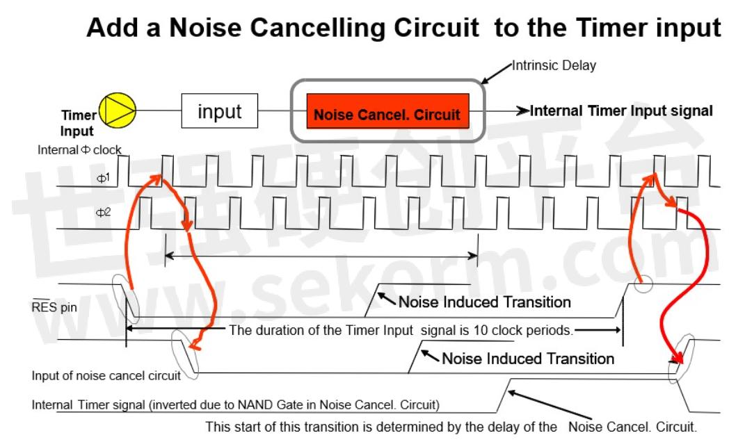
Many peripheral input pins also have programmable noise filters, these are commonly found on communication peripherals such as UART, SPI, and I2C interfaces as well as many timer inputs. The correct choice of filer clock selection is important to get the best performance out of these filters, often some trial and error are required to achieve this.

Communication interfaces are one of the biggest problem areas of a typical microcontroller design, as by nature, they are connected to the outside world and often bring high-speed signals into the system. Great care should be taken here, and the use of external protection circuitry is often advisable depending on the nature of the external environment.
We have discussed the importance of good clock system design before in a previous blog titled "Creating Reliable Crystal Oscillators Circuits for Your MCU Design", but again we would like to emphasize that it’s very important if you are using external crystals, to make sure they are correctly matched to your PCB design and to the device. This is especially true if you are using a low-speed, 32kHz oscillator, as these are notoriously prone to problems in noisy environments. We always recommend you check with your oscillator supplier for the correct matched circuit to operate with our devices. A stable oscillator circuit with a lot of margins is much less likely to cause problems.
Watchdog timers are an excellent method of recovering your application when noise causes a system's crash, However, it’s important to consider how to use these correctly.
On RA microcontrollers, watchdog timers come in two flavors, the standard watchdog timer which can be clocked from a number of the standard clock sources on the microcontroller. This watchdog is typically used to check the application’s code execution and to detect any malfunction or unexpected operation. It’s typically switched off during low-power applications. This watchdog can generate a RESET or an interrupt when it times out.

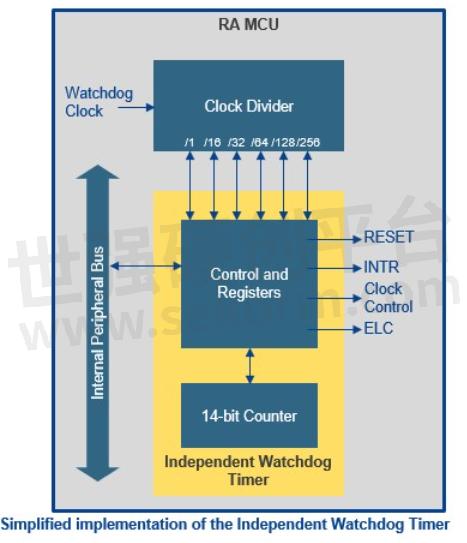
The second watchdog timer is the Intelligent Watchdog Timer (iWDT), this WDT uses a dedicated low-speed on-chip oscillator as its clock source allowing a long time out and also allowing independent operation from the normal CPU clocks, so even if the CPU clock fails, the iWDT will still cause a reset or an interrupt after it times out. A simplified block diagram of the iWDT is shown above.
Each of the watchdogs can operate with a "window" function, where a "tickle" that occurs too early as well as the watchdog timing out can cause a reset. Each watchdog can be selected to auto-start after a reset by setting the relevant bits in the option function select register, a flash-based register that holds initialization data for the device.
A common mistake we often see is to place the watchdog "tickle" inside an interrupt service routine, as this is considered efficient, as only one instance is normally required. However, this can be dangerous, as while the main application may crash, the interrupt system may continue to operate, so negating the watchdog.
When your application is complete, you should analyze all the possible execution paths. This can be difficult for complex applications using an OS, but modern code analysis tools integrated into modern development tools can help here.
Then you should place multiple instances of the watchdog tickle at relevant locations throughout the application, this will make the application much more reliable, and have the added advantage that it will detect if the application takes an unexpected execution path which is normally an indication of a serious issue such as a system rash or a pointer overflow.
We’ve already mentioned low-power applications, and the use of watchdog timers in low-power applications also needs special consideration. You should consider carefully what happens when the system is placed in low power.
These are just some of the features of our RA microcontrollers that are designed to make your system more reliable. In previous Reducing Noise Issues in Microcontroller Systems blogs, we have covered functions such as the Data Operating Circuit and the ECC SRAM which can also be used to make your systems more reliable in a noisy environment by detecting if there is some problem with the on-chip memory. We also have features such as Trustzone® and the on-chip Memory Protection Units, which can be used to detect unauthorized or unexpected access to secure memory and peripherals which can also be an indication of systems failure.
I hope you’ve found this blog useful and have pointed you to some of the features in our devices that may help you make a more reliable application.
- |
- +1 赞 0
- 收藏
- 评论 0
本文由叫我大表哥吧转载自Renesas blogs,原文标题为:Reducing Noise Issues in Microcontroller Systems - Part 4,本站所有转载文章系出于传递更多信息之目的,且明确注明来源,不希望被转载的媒体或个人可与我们联系,我们将立即进行删除处理。
相关研发服务和供应服务
相关推荐
【经验】CS+开发瑞萨MCU RH850的ADC+DMA调试指引
Renesas的RH850 F1K是汽车车身控制的首选MCU,由于高性能和安全性得到汽车客户认可,但由于开发资料有限,导致许多客户开发比较头痛。近期有客户在使用DMA的开发中遇到了问题,下面结合F1K的开发板实现ADC+DMA的驱动设计。
【经验】关于瑞萨MCU RH850的option bytes配置说明
瑞萨MCU RH850比较特殊的地方,其中一点就是Option Bytes配置。Option Bytes实际上是一个扩展区域,用于保存用户上电初始化配置的参数。我们以RH850 F1L系列为例。
【经验】e2studio调试瑞萨MCU stack栈设置及查看
近期有客户使用e2studio调试瑞萨(Renesas)MCU时,需要查看栈的使用情况,通过软件找了一圈没有发现,感觉是没提供这个功能。其实e2studio是有的,本文介绍stack栈的调试窗调出。
世强目前有代理riscv的mcu吗?
世强代理的RISC-V内核MCU厂家越来越多,还在不断增长。 国外厂家有瑞萨 【产品】瑞萨推出全新RISC-V MCU R9A02G020,优化先进电机控制系统设计和降低用户开发成本 国内厂家介绍如下: 广芯微内置32位RISC-V内核的PD SoC芯片UM3506,最高主频33MHz 全球首家全栈自研RISC-V内核的通讯接口芯片/全栈MCU供应商沁恒(WCH) RISC-V内核低功耗32位MCU,中移芯昇授权世强先进全线代理 芯昇科技携多款芯片产品亮相ICDIA,助力RISC-V生态发展 先楫半导体提供多系列通用MCU,以开源的RISC-V架构为核心,综合性能达世界领先水平 航顺芯片首次进入胡润全球独角兽榜,已量产中国第一颗M3+RISC-V多核MCU 中微半导体积极推动RISC-V架构安全化、智能化,共筑国产安全芯片生态 博流业界第一款基于RISC-V CPU的WI-FI+BLE双模SoC芯片,打造智慧家居AIoT芯片平台 璇玑CLE系列是核芯互联基于32位RISC-V内核推出的通用嵌入式MCU处理器 方寸微电子加入RISC-V产业联盟,推动安全芯片国产化,打破国外芯片技术垄断
RL78/G24瑞萨MCU
型号- R7F101GBE,R7F101GBG,R7F101G7G2DNP,R7F101GBG4CNP,R7F101GJE,R7F101G7G4CNP,R7F101GJG,R7F101GBG2DNP,R7F101GFE,R7F101GEE3CNP,R7F101GFG,R7F101GJE3CFA,R7F101GBG2DFP,R7F101GAE3CSP,R7F101GFE3CFP,R7F101G7E4CNP,R7F101G7E2DNP,R7F101GEE4CNP,R7F101G7G3CNP,R7F101GAG3CSP,R7F101GFG3CFP,R7F101GBE2DNP,R7F101GBE4CNP,R7F101GGE,R7F101GEE2DNP,R7F101GGE4CFB,R7F101GGG,R7F101GBE2DFP,R7F101GJE2DFA,R7F101G7E3CNP,R7F101GJE4CFA,R7F101G6E,R7F101G8E3CLA,R7F101G8G2DLA,R7F101G6G,R7F101GGG3CNP,R7F101GAG2DSP,R7F101GFG2DFP,R7F101GAG4CSP,R7F101GGE2DNP,R7F101GLG3CFA,R7F101GLG,R7F101GGG3CFB,R7F101GLG3CFB,R7F101GLE2DFB,R7F101GEG4CNP,R7F101GLE2DFA,R7F101GBE3CNP,R7F101GEG2DNP,R7F101GGE2DFB,R7F101GBE3CFP,RL78/G24,R7F101GLE,R7F101GJG4CFA,R7F101G6E2DSP,R7F101G8G3CLA,R7F101G6E4CSP,R7F101G8E2DLA,R7F101G6G3CSP,R7F101G7E,R7F101G7G,R7F101GGG2DNP,R7F101GEG,R7F101GAE,R7F101GAG,R7F101GEG3CNP,R7F101GGE3CNP,R7F101GJG2DFA,R7F101GFE2DFP,R7F101GLE3CFB,R7F101GLG2DFB,R7F101GGG4CFB,R7F101GLE3CFA,R7F101GLG2DFA,R7F101GBG3CNP,R7F101GLL3XXXCFB#AA1,R7F101GGE3CFB,R7F101GGG2DFB,R7F101GEE,R7F101GAE4CSP,R7F101GJG3CFA,R7F101GBG3CFP,R7F101G6G4CSP,R7F101G8E,R7F101GAE2DSP,R7F101G8G,R7F101G6G2DSP,R7F101G6E3CSP
【经验】瑞萨RA系列MCU使用e2 studio的断点调试方法和注意事项
瑞萨RA系列MCU可以使用e2 studio等开发环境进行调试和下载程序,在使用e2 studio时我们经常会遇到一些异常现象,如没有办法下断点进行调试,无法debug观察寄存器状态等,本文将介绍一下e2 studio常见的断点调试方法和注意事项。
RA系列MCU注入电流,防止损坏MCU应用笔记
描述- 本资料介绍了如何防止RA系列微控制器(MCU)因异常注入电流而损坏。内容包括推荐的注入电流条件、不同型号的参数限制以及额外的说明和建议,旨在指导用户在设计和应用过程中采取适当的措施以保护MCU免受损害。
型号- RA FAMILY,RA4T1,RA6T2,RA6T1,RA6T3,RA4M1,RA2L1,RA4M3,RA6M1,RA4M2,RA6M3,RA6M2,RA6M5,RA2E1,RA6M4,RA4E1,RA2E2,RA6E1,RA2A1,RA4E2,RA6E2
【经验】基于MCU CS+ RH850/F1K Boot开发指引
车载ECU开发都需要通过Boot实现在线升级,Boot是嵌在APP前面执行的程序,在需要更新APP代码时会对flash APP部分重新编程。近期有客户调试RH850/F1K MCU出现Boot跳到APP程序不能执行,下面以开发板为例实现Boot到APP。
【经验】解析瑞萨RA家族MCU的主要区别及命名规则
目前瑞萨电子(Renesas)已经发布的RA产品家族MCU主要包括四个系列即RA2系列、RA4系列和RA6系列,以及计划发布的RA8系列。有很多客户不了解RA家族处理器的主要区别和命名规则,本文讲详细讲解。
【经验】瑞萨RA MCU CAN和CANFD IP介绍
目前RA MCU提供以上三种CAN&CANFD IP,如果需要在CAN总线上添加CAN节点,以上三种CAN&CAN IP均可;如果需要在CAN总线上添加CANFD节点,请选择CANFD或者CANFD Lite;如果需要用到2个通道,请选择RA6M5的CANFD。
【经验】瑞萨RA系列MCU在Keil开发环境下的开发介绍
本文主要介绍在Keil环境下如何新建瑞萨RA项目工程以及在已存在的RA醒目工程中如何通过图形化工具进行代码的底层配置。
【经验】关于瑞萨MCU RH850 C1M-A2的内存地址分配介绍
本文是关于瑞萨MCU RH850 C1M-A2的内存地址分配介绍,我们在设计瑞萨MCU RH850 C1M-A2的时候,对内存空间分布一定要有所了解。芯片内部flash和ram空间大小如下。
【经验】瑞萨MCU RA6M4 USB转串口调试指引
USB现已非常普及,在小小的单片机上都可以实现,瑞萨的RA6M4是基于Armv8-M架构的Arm®Cortex®-M33内核MCU,其接口非常丰富,就带有USB接口。以往的USB开发给人非常繁琐的感觉,现通过e2 studio开发变得非常简单。
【经验】MCU RH850/F1K舵机PWM调试分享
PWM常常作为电机控制、舵机控制等使用,也是开发中最常用的控制方式。PWM实现需要使用定时器,RH850有非常多的定时器,并且可以配置很多通道,下面以瑞萨MCU RH850/F1K的TAUJ0定时器作为PWM定时器,实现PWM输出。
【经验】瑞萨RA系列MCU低功耗唤醒功能测试
瑞萨RA系列MCU低功耗一共有三种模式,本次测试选择时钟为32.76kHZ,使用电容触摸按键唤醒,datasheet上描述芯片常温下功耗为0.55uA,用开发板实测功耗为60uA,经过检测,功耗主要来源于电容电阻,开发板中有一颗电阻功耗在30uA,并具体分析。
电子商城
现货市场
服务
可定制显示屏的尺寸0.96”~15.6”,分辨率80*160~3840*2160,TN/IPS视角,支持RGB、MCU、SPI、MIPI、LVDS、HDMI接口,配套定制玻璃、背光、FPCA/PCBA。
最小起订量: 1000 提交需求>
拥有IC烧录机20余款,100余台设备,可以烧录各种封装的IC;可烧录MCU、FLASH、EMMC、NAND FLASH、EPROM等各类型芯片,支持WIFI/BT模组PCBA烧录、测试。
最小起订量: 1 提交需求>


登录 | 立即注册
提交评论