ATP‘s PCB Assembly Solderability Validation Tests


Overview of ATP’s PCB Assembly Solderability Validation Tests
Soldering is an important process to make sure that components on the printed circuit board assembly (PCBA) are effectively bonded to form reliable mechanical and electrical connections. Part of this process is called “wetting,” where the metal in the solder becomes molten fluid to bond and adhere with the metal components on the PCB. Evaluating solderability is the process of testing how well the solder secures those connections. This crucial process must be done before finalizing the PCB assembly, as poorly soldered parts can affect the PCB functionality, lead to defects, and incur more costs.
ATP PCB Assembly Solderability Validation
ATP performs solderability validation using temperature stress and external forces to validate the robustness of the soldering process.
The tests included in the solder process validation are described in this section.
Visual Inspection
●Automated Optical Inspection (AOI) – Typically performed after the soldering process, AOI is a non-contact method where a camera autonomously scans the PCB for surface defects, soldering flaws, and missing skewed, faulty, or misplaced components.
Pass/Fail Criteria: IPC-610 Specifications
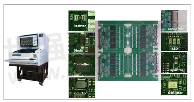
Figure 1. PCB items to be checked.
●Automatic X-Ray Inspection. Checks the solder joints are under components, which may not be visible to ordinary optical inspection equipment.
Pass/Fail Criteria: <25% void (IPC J-STD-001), open/short circuit check, component placement, solder ball size/shape check
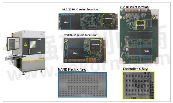
Figure 2. X-Ray Test Equipment simplifies the complex inspection of multi-layered assemblies.
●In-Circuit Test. Accesses the board’s circuit nodes and measures component performance using power parameters such as resistance and capacitance.
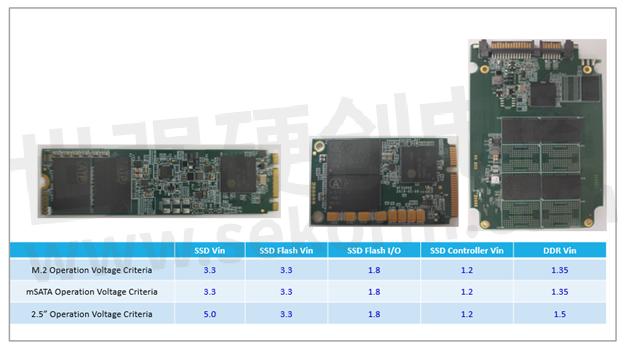
Table 1. Sample In-Circuit Validation Test results for M.2, mSATA, and 2.5” SSDs
●SSD Functional Test Verification. Uses the ATP Gym & Coach System to verify PCB functionality after burn-in using Read-Write test patterns on SSDs.
Test Benchmark: ATP Gym & Coach System
Test Condition: 10 full SSD capacity loops
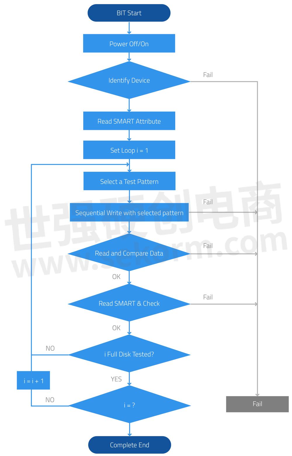
Figure 3. SSD Functional Test Process Flow
●Thermal Cycling Test. This test is used to determine the PCB’s resistance to extreme temperatures. By thermally stressing the PCB solder balls, flaws such as solder joint cracks, warps, lead damage, and other defects can be detected.
ATP performs the thermal cycling test between 0°C to 100 °C for 1000 cycles, with an interim check performed on the 500th cycle. The temperature is ramped up at 14°C per minute, with the PCB dwelling at each extreme temperature level for 10 minutes.
●Shock and Vibration Tests. In many embedded and industrial applications, PCBs are subjected to severe conditions, such as shock and vibration, that can damage the boards themselves or the components on them, compromising the physical, mechanical and electrical integrity of the PCB.
ATP performs these shock and vibration tests to make sure that the PCBs can endure such conditions.
●Non-Operational Random Vibration
●Non-Operational Half-Sine Shock
●Non-Operational Square Wave Shock
●Dye & Pry. This test is used to detect any defects on the solder ball and ball-to-pad interfaces. A dye is infused on the PCB, forcing the dye to penetrate cracks in the solder joints or on the PCB. The PCB is then dried in an oven to prevent the dye from smearing. The board is then mechanically pried to check for the presence of the dye in solder joints/balls or under the solder pads.
Pass/Fail Criteria: Follow IPC-A-610 specifications
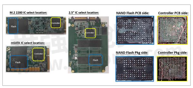
Figure 4. Dye and Pry's results on sample SSDs tested to show that there are no cracks (red dye penetration) on the solder joint and soldering ball.
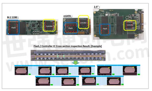
●Cross-Section Check. Also called micro-section analysis, the cross-section test inspects the internal quality of the PCB and provides an interconnection defect analysis. It helps detect internal failures, such as those related to soldering and plating, as well as the thickness of the board layers.
Pass/Fail Criteria: Intermetallic Compound (IMC) layer, soldering status check (Examples: no wetting, cold soldering, dewetting, and others)
Key Takeaways
Soldering defects can affect the functionality of the PCB assembly. This is why ATP takes great care in making sure that all PCB components are effectively bonded through the soldering process. ATP evaluates solderability through rigorous tests, such as visual inspection, thermal cycling, shock and vibration, dye and pry, and cross-section check.
ATP’s PCB assembly validation tests are part of the many reliability and endurance tests developed and performed by ATP to ensure strict compliance to the highest standards of quality. ATP is committed to delivering high-performance and high-endurance NAND flashes storage products to ensure the best value for the total cost of ownership (TCO).
- |
- +1 赞 0
- 收藏
- 评论 0
本文由深蓝的鱼转载自ATP,原文标题为:SSD PCB Assembly Solderability Validation Tests,本站所有转载文章系出于传递更多信息之目的,且明确注明来源,不希望被转载的媒体或个人可与我们联系,我们将立即进行删除处理。
相关研发服务和供应服务
相关推荐
【应用】ATP推出32G eMMC AF032GEC5X-SEK0511用于V2X系统,适用温度-40~85℃
V2X系统旨在通过允许车辆与几乎所有可检测的东西进行通讯来提高车辆的安全性,舒适性和便利性。在系统设计中需要用到eMMC进行数据存储,在此选用的ATP的32G Bytes的eMMC AF032GEC5X-SEK0511替换NAND FLASH。
ATP NVMe BGA pSLC SSD安全保护及加密功能特点
硬件写保护* 写保护功能将ATP NVMe BGA SSD置于“只读”模式,以防止数据写入设备,并保护重要数据不被意外删除、移动或修改。通过在控制器印电路板(PCB)上的通用输入/输出(GPIO)信号引脚的特定引脚上放置跳线,在存储设备上启用写保护。硬件快速擦除*对于特定应用,主机可以使用GPIO连接器触发“擦除数据”行动。
世强有关于PCIE接品的存储产品的方案介绍吗,要能做到16TB/32TB容量的,满足PCIE4。0标准。另外,这个PCB板材是否用常规的FR4即可还是说要用高频板材?请大神指点
新增工业级SSD存储、DRAM模块、NAND闪存,世强代理ATP Electronics【选型】ATP(华腾国际)内存及存储产品选型指南;【应用】ATP闪存用于IOT/IIOT中数据云存储/存储储存应用,满足严苛耐用性、保留性和可靠性要求; 高频特种多层线路PCB板打样加工服务,可提供FR4/ROGERS/ARLON/Taconic等多种板材FR-4升级替代首选Kappa™438板材,完全兼容FR-4加工工艺,兼具低成本和低损耗【选型】比传统FR-4材料高6-8倍导热系数的92ML板材,助力解决高端通信电源、工业电源的散热问题
ATP为SSD的PCB组装进行严格可焊性验证测试,确保可靠性和耐久性
ATP 通过严格的测试来评估可焊性,例如目视检查、热循环、冲击和振动、染色以及截面检查。本文描述了焊接工艺验证中包含的测试项及其验证标准。
【经验】DRAM的可靠性受什么因素影响?ATP DRAM为何具备高可靠性?
ATP的DRAM模块经过两个级别的测试,以确保最大的可靠性:1、先进的IC级集成电路测试;2、增强的模块水平测试:老化测试(TDBI)和自动测试设备(ATE)确保模块达到甚至超过合格参数。同时具有工业额定温度,采用密封涂层,使用使用抗硫电阻器(基于项目)和厚度为30µm的金手指镀层。
ATP DRAM模块选型表
ATP提供如下DRAM模块的技术选型,Technology:DDR3/DDR4/DDR5;SPEED:1600MHz~5600MHz;Capacity:4GB~16GB。
|
产品型号
|
品类
|
Technology
|
DIMM Type
|
SPEED
|
ECC
|
SIZE
|
CHIP
|
PCB Height
|
DIMM Rank
|
Pin
|
Grade
|
Operating temperature
|
|
D516G0RD568DPSC
|
DRAM MODULE
|
DDR5
|
RDIMM
|
5600MHz
|
ECC
|
16GB
|
2GX8
|
1.23"
|
1
|
288
|
CT
|
0℃~+85℃
|
选型表 - ATP 立即选型
ATP SSDs选型表
ATP推出SSDs(固态硬盘),Capacity(存储容量)120G-7680G,Operating Temperature(工作温度)-40℃~85℃
|
产品型号
|
品类
|
Product Line
|
Capacity(GB)
|
Operating Temperature(℃)
|
Power Loss Protection
|
|
FT240GP48APHBPI
|
固态硬盘
|
N651Si
|
240GB
|
-40℃~85℃
|
Hardware + Firmware Based
|
选型表 - ATP 立即选型
ATP对所有SSD进行数千小时RDT测试,确保产品严格遵守最高质量标准
可靠性验证试验(RDT)是对ATP固态驱动器(SSD)进行的一项长期严格测试,旨在证明每个SSD符合最严格的质量要求。ATP在较长时间内对其 SSD执行完整的实际驱动器级别测试,以验证额定MTBF值,而不是依赖可靠性预测系统。
ATP UHS-I microSDXC, A1, U3 Memory Card Specification
型号- FT256GUD4APEBFI-SEK1,FT64G0UD4APEBFC-SEK1,FT512GUD4APEBFI- SEK1,FT128GUD4APEBFI- SEK1,FT128GUD4APEBFI-SEK1,FT512GUD4APEBFI-SEK1,FT512GUD4APEBFC-SEK1,FT64G0UD4APEBFI-SEK1,FT64G0UD4APEBFI- SEK1,FT128GUD4APEBFC-SEK1,FT256GUD4APEBFC-SEK1,FT256GUD4APEBFI- SEK1
【技术】符合Opal 2.0的ATP SATA和NVMe™驱动器,确保静态数据安全
ATP的下一代SATA和NVMe驱动器符合Opal 2.0标准,从而确保了静态数据的安全保护层
The ATP Gym and Coach System: Exercising SSDs to Ensure Total Fitness
With the Gym and Coach system, ATP has dramatically improved RDT and the initialization process for functional test details. By making industrial SSDs undergo a lot of “painful” exercises through stringent testing, ATP makes sure that customers have everything to gain by receiving the most robust, reliable and enduring flash storage products for their applications.
ATP Exhibits at Embedded World 2024
Participants should not miss a visit to ATP’s Booth in Hall 1-210, where ATP once again demonstrates its commitment to redefine memory and data storage reliability, scalability, and efficiency. Attendees to Embedded World 2024 can expect to see a new breed of flash storage solutions with ATP’s 176-layer NAND flash innovation, industrial enterprise-readiness for Edge computing and artificial intelligence, and latest DDR5-5600 memory offerings.
电子商城
现货市场
服务
采用SMT/SMT+DIP封装加工,PCB成品尺寸:50*50~340*500mm,板厚:0.6~3.0mm,最快交期:2~3天。支持1~200片(拼版200片)的PCBA主板贴片。
最小起订量: 1 提交需求>
可加工PCB板层数1~40,最小线宽/间距内层: 2.5/3mil (H/H OZ base copper);最小线宽/间距外层: 3/3mil (H/H OZ base copper);成品交货尺寸范围:10 * 10mm~570 * 1200mm。板厚范围:0.4mm-10mm。支持通孔板、HDI板、柔性板、刚柔结合板打样、小批量及批量生产。
最小起订量: 1 提交需求>


登录 | 立即注册
提交评论