Intellectual Power Amplifier Module Based on GaN FETs


In the past few years, gallium-nitride (GaN) FETs have become more widespread in power electronics. Due to their outstanding characteristics, GaN FETs play an increasingly important role in the miniaturization of the switching converters with very high-power densities exceeding 100 W / cm3 and more. The efficiency of converters based on GaN transistors can reach 99.5%. Due to the extension of the conversion frequency towards the MHz range, the magnetic components (chokes, transformers) also decrease in size significantly. However, designers face numerous challenges in implementing practical GaN transistor designs. The best family members are presented in a wafer-level chip-scale package; the drivers are also quite miniature.

There is a significant problem in optimizing the gate control circuit and its topology due to extremely fast switching speed. As a reminder, GaN FETs have no familiar parasitic body diodes which affect the application design. Taking into consideration the values of the currents and voltages, relative to the size of the power elements, it becomes clear that a new design approach is needed in terms of the PCB topology, heat dissipation, and ensuring the safe area operation for all working modes. As usual, the designer must choose two of three between "Cost", "Efficiency" and "EMC", but for GaN FETs this combination is extended compared to Si MOSFETs.
To simplify and accelerate the development process of many devices (D-class audio amplifiers, AC current and voltage calibrators, power supply modulators, etc.), the idea of creating an Intellectual Power Amplifier Module (IPAM) with the following parameters appeared:
• Supply voltage up to 80 V, output current up to 20 A
• Sinusoidal output power 500 watts
• Efficiency 98% (half power), 96% (rated power)
• Full Power Bandwidth 0…50 kHz
• Main carrier frequency 1 MHz, internal transitions up to 10 MHz
• Less than 0.01% THD (-1dB)
• Diagnostics and parameter setting via 2-Wire Serial Interface (TWI)
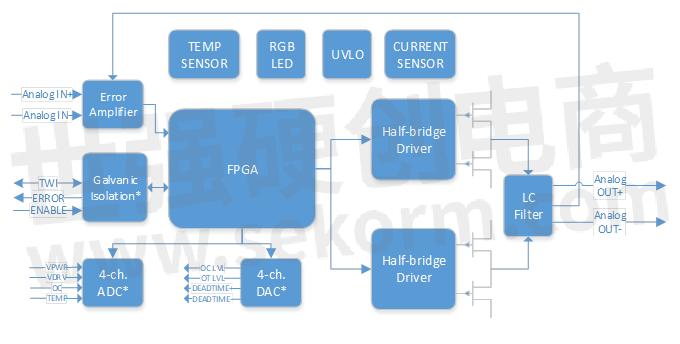
IPAM is a fully differential pulsing power amplifier covered by common negative feedback. Typical carrier frequency is approximately 1 MHz and may vary within ±50 % based on the input level, output power, and load impedance. A high-speed precision comparator is used as an error amplifier.

The module contains a small FPGA chip. The first important FPGA function is to produce additional pulses for the best amplifier linearity. The second FPGA function is to maintain safe operating modes of the power switches and the output choke, regardless of the parameters of the input analog or PWM signal. FPGA limits the modulation index and some other parameters. When the transition frequency drops below the limit, the FPGA generates extra pulses that prevent the UVLO detector from triggering due to the discharge of bootstrap capacitors. The minimum pulse length is also limited to comply with the driver circuit possibilities. If the parameters of the input signal corresponding with the introduced restrictions, the pulse sequence from error amplifier output are transmitted asynchronously to the half-bridge drivers, with a delay of fewer than 5 ns and minimal time distortion. All parameters are programmable via TWI and can be deactivated by the user.
IPAM has no dependency on THD+N vs Frequency and has a very low dependency on THD+N vs Output Power thanks to its original control loop structure. For output power up to 200-250 W RMS, IPAM does not require an additional heatsink for generic scenarios.

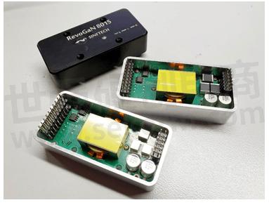
The problem of heat removal is solved by using a six-layer PCB with 35 µm Cu on the outer layers and 70 µm on the inner layers, and the vias are filled with copper. The module is housed in a CNC-machined aluminum enclosure with 76 x 36 x 18 mm dimensions. At the last stage, vacuum filling is performed with a specialized ceramic-based compound with very high thermal conductivity.

The development of the output choke has turned into a separate R&D work related to the need to study the parameters of the newest high-frequency power ferrites manufactured by TDK/EPCos and Ferroxcube. Unfortunately, these companies did not provide sufficient data for accurate calculations. I had to find a way to make samples with different gaps and different numbers of turns and study them in detail. It took more than one month with the corresponding costs.
As a result, 33 μH small-sized chokes with a 20 A linear current range and SRF > 10 MHz were created. Unfortunately, the world industry does not produce chokes with similar characteristics. I have got about 16 usable chokes with different parameters.
I also had to study the real characteristics of various film capacitors for the output demodulating LC filter and opt for products with a polyphenyl sulfide dielectric. Ceramic capacitors are not suitable for these purposes due to their enormous nonlinearity. Special attention was paid to choose optimal ceramic blocking capacitors for the power stage. I am not sure if I could do this work without Vector Network Analyzer, 2 GHz Oscilloscope with active probes, and a couple of burning experiments at the start. Many reference designs are "thing in itself" and can work only “as is” on your lab table but do not work in a real environment, especially if they are tied up by external connections which produce EMI problems. I managed to achieve that almost all high-frequency components of the switching current circulate inside the module.
Please carefully design the gate driver circuit if you want to achieve high efficiency and do not want to have EMI problems in the future. I highly recommend simulating the circuit by adding parasitic inductances before you start to burn it naturally. With GaN FETs, there is a very thin trade-off between reliable gate control and practical parameters (Efficiency, EMI). It is possible to find a way to keep confident control of the gate. I propose to use several wonderful properties of ferrite beads which can be used for some non-trivial cases. Due to the extremely high dV/dt and dI/dt, significant voltage spikes occur between the power and signal grounds of the module during operation. I added galvanic isolation for TWI and ERR/ENA control signals.
The RGB LED indicates the fact and cause of multiple failures. The types of errors are encoded in series of flashes separated by a long pause. IPAM can be re-initialized automatically, using the built-in timer that generates the protective interval.
A general-purpose 2-phase module without an output demodulating filter is under development. It can be used for a wide range of DC/DC converters with different topologies (buck-, boost- or LLC). A 3-phase version of the power module with similar parameters can be built.
I would like to express my gratitude to EPC European office for the timely support. The result of this big two years’ work is a deep understanding of the capabilities of GaN power electronics. Several architectural, circuitry, topological and design solutions have been developed, which now make it possible to develop a wide range of various devices for breakthrough electronic systems.
- |
- +1 赞 0
- 收藏
- 评论 0
本文由董慧转载自EPC,原文标题为:Intellectual Power Amplifier Module based on GaN FETs,本站所有转载文章系出于传递更多信息之目的,且明确注明来源,不希望被转载的媒体或个人可与我们联系,我们将立即进行删除处理。
相关推荐
EPC eGaN®FET/晶体管选型表
EPC提供增强型氮化镓半桥功率晶体管/增强型功率晶体管/功率晶体管的选型:配置:Dual Common Source、Dual with Sync Boot、Half Bridge、Half Bridge Driver IC、HS FET + Driver + Level Shift、Single、Single - AEC Q101、Single – Rad Hard、Single with Gate Diode、Single with Gate Diode – AEC-Q101、Dual Common Source - AEC Q101,VDS最大值(V):15~350V;VGS最大值(V):5.75~7V
|
产品型号
|
品类
|
Configuration
|
VDSmax(V)
|
VGSmax(V)
|
Max RDS(on) (mΩ)
@ 5 VGS
|
QG typ(nC)
|
QGS typ (nC)
|
QGD typ (nC)
|
QOSS typ (nC)
|
QRR(nC)
|
CISS (pF)
|
COSS (pF)
|
CRSS (pF)
|
ID(A)
|
Pulsed ID (A)
|
Max TJ (°C)
|
Package(mm)
|
Launch Date
|
|
EPC2040
|
Enhancement Mode Power Transistor
|
Single
|
15
|
6
|
30
|
0.745
|
0.23
|
0.14
|
0.42
|
0
|
86
|
67
|
20
|
3.4
|
28
|
150
|
BGA 0.85 x 1.2
|
Apr, 2017
|
选型表 - EPC 立即选型
【视频】EPC氮化镓产品在DCDC的应用,可减少损耗
描述- Efficient Power Conversion (EPC) 作为全球领先的功率转换技术供应商,提供基于氮化镓 (GaN) 的场效应晶体管 (FET) 和集成电路 (IC)。EPC 的 GaN 基器件具有高效率、快速开关速度、小型化和低成本等优势,广泛应用于消费电子、通信、汽车和可再生能源领域。资料中详细介绍了 GaN 基 DC-DC 转换器,包括企业电源架构、功率密度、EPC9159 转换器规格、转换器概述、特色 GaN FET 以及效率与损耗测量等。此外,还讨论了 GaN FET 在提高功率密度和简化设计方面的优势。
型号- EPC2302,EPC2305,EPC2308,EPC23101,EPC23102
EPC 9176_B5345_第3版_0
描述- 这份资料主要涉及元器件行业中的多种电子元件及其应用,包括电容、电感、二极管、晶体管等。资料中详细介绍了不同类型元件的规格、参数和应用场景,如PIC9201电容、PIC9202电感等。此外,还涉及了电源转换、温度传感、电流传感等方面的设计实例,如AP1065_5V2_100mA_0805电源模块、AP1009_0805_2p3V电源模块等。
型号- EPC9176
EPC Altium库PCBLIB&SCHLIB&INTLIB
型号- EPC2212,EPC2214,EPC2012C,EPC2059,EPC2216,EPC2215,EPC2218,EPC2016C,EPC2019,EPC2050,EPC2052,EPC2051,EPC2054,EPC2252,EPC2053,EPC2055,EPC2218A,EPC2069,EPC2102,EPC2024,EPC2101,EPC2104,EPC2302,EPC8009,EPC2001C,EPC2103,EPC2029,EPC2106,EPC2304,EPC2105,EPC2108,EPC2306,EPC2107,EPC2305,EPC8002,EPC2021,EPC2065,EPC2020,EPC2023,EPC2067,EPC2100,EPC21701,EPC2221,EPC2022,EPC2066,EPC8004,EPC2219,EPC2619,EPC2036,EPC2010C,EPC2035,EPC2038,EPC2034C,EPC2037,EPC2014C,EPC2039,EPC2071,EPC23101,EPC2030,EPC23102,EPC23103,EPC2032,EPC23104,EPC2031,EPC2152,EPC2111,EPC2033,EPC2110,EPC8010,EPC2204A,EPC2070,EPC2308,EPC2307,EPC2203,EPC2202,EPC2204,EPC2015C,EPC2207,EPC2206,EPC2007C,EPC2040,EPC21603,EPC2045,EPC2044,EPC2088,EPC21601
无锡恒芯微LED非隔离芯片选型表
无锡恒芯微提供以下技术参数的LED非隔离芯片选型,典型效率为80~93%,功率因数:>0.5~>0.9,输入电压为90V~265V,有多种封装方式,功率范围大。
|
产品型号
|
品类
|
封装
|
功率范围(W)
|
典型应用
|
输入电压(V)
|
功率因数
|
典型效率
|
|
HA5831E
|
LED非隔离驱动器
|
SOP8
|
1~7W
|
80mA@80V
|
120~265Vac
|
>0.5
|
92%
|
选型表 - 无锡恒芯微 立即选型
EPC交叉引用搜索快速入门指南
描述- EPC与DiscoverEE合作推出EPC GaN Power Bench工具,提供基于超过20,000个MOSFET的数据库,方便设计师和采购人员查找替代器件。工具基于实际损耗计算,提供参数比较和损耗分析,支持生成永久链接分享结果。
型号- BSC320N20NS3 G
EPC评估套件选型表
EPC提供评估板的选型:Default Configuration:IToF、Resonant Pulse DToF;VBUS (max)(V):12~160V;VINPUT(max)(V):5 V;Tpin(min)(ns):1 ns/2 ns
|
产品型号
|
品类
|
Description
|
VIN(V)
|
VOUT(V)
|
IOUT (A)
|
Featured Product
|
|
EPC9163
|
评估板
|
Synchronous, Buck or Boost, digital controller
|
Buck: 20 – 60 V
Boost: 11.3 – 16 V
|
Buck: 5 - 16 V
Boost: 20-50 V
|
140 A (Buck)
|
EPC2218
|
选型表 - EPC 立即选型
FM13UF011x EPC Gen2 UHF标签芯片规格书
描述- 本资料为上海复旦大学微电子集团股份有限公司生产的FM13UF011X超高频标签芯片的数据手册。该芯片符合EPC全球Class1 Gen2V2和ISO/IEC 18000-63(Type C)标准,具有双差分射频端口,适用于库存管理、供应链管理、人员或车辆识别等领域。
型号- UF011X,FM13UF011X-041-WTBU2-C,FM13UF011X-040-WTBU2-C,FM13UF011X-XXX-XXXXX-X,FM13UF011X
Littelfuse(力特)中央电气控制盒 EPC 数据手册
描述- 该资料介绍了Littelfuse和Colehersee生产的中央电气控制盒EPCRev 01,一款适用于汽车和其他工业应用的电子控制单元。它具有小型化设计、高集成度、多种接口选项和IP67防护等级等特点。
型号- EPC
EPC氮化镓晶体管选型表
EPC提供以下氮化镓功率晶体管/GaN功率晶体管选型,最大耐压15V-350V,持续电流0.5A-90A,导通阻抗1.45Ω-3300mΩ,导通电荷0.044nC-19nC,峰值电流0.5A-590A。
|
产品型号
|
品类
|
最大耐压(V)
|
持续电流(A)
|
导通阻抗(mΩ)
|
导通电荷(nC)
|
峰值电流(A)
|
封装(mm)
|
|
EPC2040
|
Enhancement Mode Power Transistor
|
15V
|
3.4A
|
30mΩ
|
0.745nC
|
28A
|
BGA 0.85 mm*1.2mm
|
选型表 - EPC 立即选型
EPC系列可配置内部总线密封配电模块
描述- 本资料介绍了EPC系列内部总线密封电源分配模块(PDM),这是一种可配置的汽车级电力分配解决方案,适用于商业车辆的电气系统。该模块具有高功率电路密集设计,支持插件式设备,包括保险丝、断路器、二极管和继电器,以保护和控制复杂的电气系统。
型号- EPC SERIES,LFLX0006Z-01,EPC
EPC半桥Demo选型表
EPC提供半桥Demo选型:VDS(最大值)(V):20V~350V,Id(RMS最大值)(A):1A~65A
|
产品型号
|
品类
|
Description
|
VDS max(V)
|
ID(max RMS)(A)
|
Featured Product
|
|
EPC9086
|
开发板
|
Half Bridge Plus Driver
|
30
|
15
|
EPC2111
|
选型表 - EPC 立即选型
电子商城


登录 | 立即注册
提交评论