Inductance Optimization for Laminated Busbars


The stray inductance of switching circuits is one of the most critical parameters in the design of power electronics and is becoming even more important for systems using wide-bandgap semiconductors, such as SiC and GaN.
The operating principle of power electronics is based on switches (the semiconductor devices) commutating at frequencies in the order of kHz to create low frequency or DC power. When a switch changes its state, it must deal with the voltage and current in the circuit. For example, in the case of ON to OFF switching, the current flowing in the switch tends to continue flowing which can be regarded as electric inertia or inductance. When this current reaches the closed switch it “crashes” into it like a wave into a breakwater wall, creating a spike in voltage. Thus, the higher the inductance the higher the voltage surge in the semiconductors. In fact, this phenomenon is analog to a water hammer where the speed of liquid flowing in a pipe transforms into an overpressure when we close the tap (that is why any plumber would advise to always close the taps gently).
There are other negative effects linked to the inductance of power circuits, such as EMI (electromagnetic interference). For a given current, a high inductance is a consequence of high unrestrained magnetic flux and can be reduced by correctly routing and shaping the conductors.
Here is where Laminated Busbars come into play: the inductance of a conductor depends on its shape, the proximity of the current paths, and the lowest inductance geometry given by parallel planes: exactly the structure of a busbar. When required to reduce inductance to a minimum, the laminated busbar brings conductors extremely close to each other, in some cases under 100µm.
The inductance of a pair of wires 1 mm apart and 1m in length is around 0.4 mH. It may seem to be a low value but for power electronics, the required inductance is in the range of the nano Henries. The equivalent construction in a busbar of the same section would be 50 nH which is already 88% lower. Additionally, if the distance between conductors is reduced by high-end insulation, for example, 0.2mm, inductance is reduced to below 20 nH.
This was an ideal case to show the potential of busbar construction and the calculations that can be performed using simple formulas. In a real application, the shape of a busbar is much more complex and must comply with many other requirements such as connection points (to semiconductor devices, to capacitors, to power cables, or other busbars), insulation for the required voltage level, adequate thermal dissipation, fixation elements, and of course manufacturability.
Inductance measurement of real busbars has traditionally been performed by lab or field testing. It requires highly specialized equipment and a delicate setup. Additionally, at least one prototype must be manufactured. The effect of small changes in the geometry of the busbar can have a large impact on the inductance, therefore it is extremely difficult to build a sample that can be modified for testing and optimization. However, Finite Element Method simulations do not require a physical sample and modifications can be easily done in the 3D model of the busbar. This allows a fast-iterative process that translates into a very low inductance solution. Furthermore, other features of the busbar can be evaluated in parallel by FEM simulations such as current distribution and thermal behavior which leads to a highly optimized busbar. When a busbar is simulated to evaluate its inductance a plot of the magnetic field is obtained. As mentioned before, the inductance is proportional to the magnetic field. Besides, a simulation allows a fast sweep along with a wide range of frequencies, reaching up to MHz. This is especially valuable as magnetic flux is highly dependent on the frequency and each system is designed for a particular switching frequency and slope. Consequently, due to the simulation results, it is easy to pinpoint the most critical areas for improvement and act on them.
In the following paragraph, it will be demonstrated how a typical inductance optimization is performed.
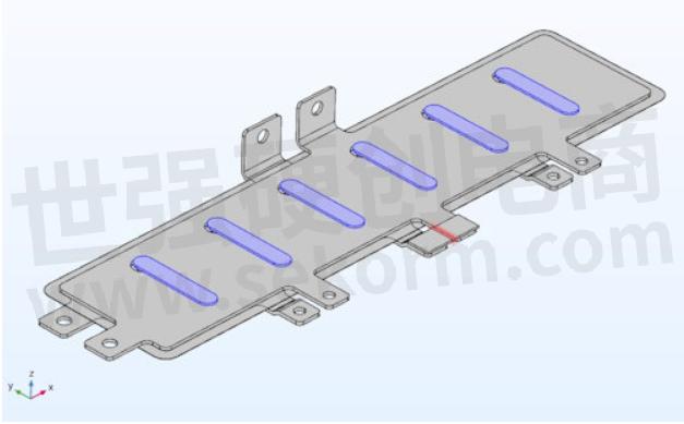
The first step is to 3D model the busbar that shall be simulated. Typically, semiconductor devices and capacitors are not included in the model. The capacitors are substituted by a short-circuit that allows current to flow following the lowest-impedance path. In order to calculate this path simulation software considers all electromagnetic physics constraints, including proximity and skin effect at high frequencies. In the connection of the semiconductor devices, the probe to evaluate the inductance is placed.
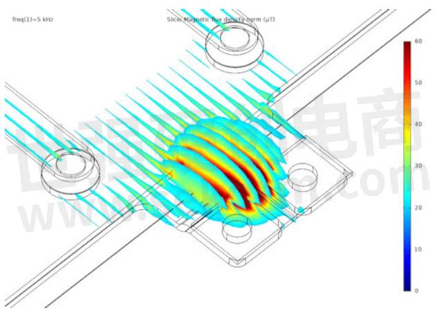
The next image shows the 3D model of the first busbar design. The elements highlighted in blue are the short-circuit blocks at the capacitor positions and the red element is the probe which is placed at the connection of the central IGBT in this case.
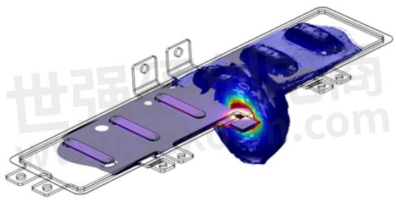
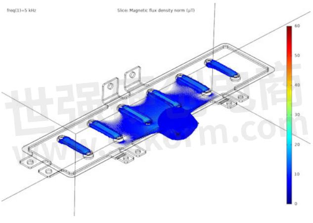
The simulation shows the areas in and around the busbar with a high magnetic flux (values in µT, as probe current, is only 1 A). It can be observed that the highest magnetic flux, thus the largest contribution to the inductance is found in the connection terminal of the IGBT. The second-largest contributors are the capacitor connections.
The total inductance of this system at the simulation frequency of 5kHz is 12.0 nH.
When zooming into the terminal area it is noted that the magnetic flux is created in the open-loop between the terminals. Thus, why it is highly recommended to optimize this part to have a large impact on the inductance reduction.
The first optimization consists of changing the bend terminal from the original design into a flat terminal with connection bushings. This allows to reduce the open gap and decreases the inductance to 9.2 nH.
In a second optimization loop, the overlap between the terminals is increased, which reduces the flux in the area. As a result, the inductance is further reduced to 4.5 nH.
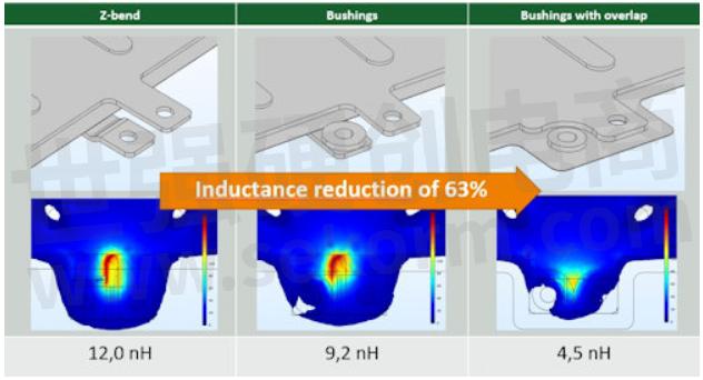
The optimization could continue and tackle other areas of the busbar, but it has been demonstrated that with a fast approach the inductance of the original part has been reduced by 63% to a value below 5 nH. With the right tools, knowledge, and experience FEM simulation is an ideal approach to optimize the inductance of a laminated busbar (which is, by construction, the lowest inductance structure) in order to boost the performance of any power electronics system.
- |
- +1 赞 0
- 收藏
- 评论 0
本文由董慧转载自Rogers,原文标题为:Inductance Optimization for Laminated Busbars,本站所有转载文章系出于传递更多信息之目的,且明确注明来源,不希望被转载的媒体或个人可与我们联系,我们将立即进行删除处理。
相关推荐

Rogers Corporation’s Curamik® Ceramic Substrates, Low Inductive ROLINX® Laminated Busbars Power Renewable Energy Sources
The 2024 Paris Summer Olympic Games have captivated audiences worldwide, and part of that excitement has centered around the new and innovative technology applications utilized in this year’s games. Many of these technologies are enabled by materials that Rogers Corporation manufactures, including applications in footwear, 5G wireless infrastructure, renewable energy, and more.

Busbars for e-Aviation and High Altitude Applications
The evolution to cleaner transportation is pushing the development of e-aircrafts and is already reality in development phase. Operation at high altitude and other demanding specifications creates many challenges, pushing all electrical components a step further in performance. Operating at high altitude with low air density has many implications on the design of laminated busbars. Technical requirements, ambient conditions and physical phenomena are studied case by case at Rogers to deliver the safest and most optimized ROLINX busbar solution.

Rogers Announces Termination of Merger Agreement with DuPont
Rogers announced the termination of its definitive merger agreement with DuPont de Nemours, Inc. (“DuPont”). In connection with the termination of the merger agreement, Rogers has received a regulatory termination fee of $162.5 million from DuPont.

ROLINX®性能产品信息
ROLINX® Performance 是一种多层母线产品,适用于高功率应用。该产品结合了多年的制造经验,专为处理数千伏工作电压和超过1000安培电流的电力分配系统而设计。它提供优化的电感、控制局部放电水平,并支持高效的设计。
ROGERS - LAMINATED BUSBARS,叠层母线,ROLINX® PERFORMANCE,通信基础设施,医学,COMMUNICATION INFRASTRUCTURE,清洁能源,国防和航空航天,混合动力汽车/电动汽车,PROPULSION SYSTEMS (MASS TRANSIT, SHIP PROPULSION, MINING VEHICLES, ETC.),DEFENSE AND AEROSPACE,PROCESS AND AUTOMATION,HVDC / SMART GRID,工业转换器,INDUSTRIAL CONVERTERS,HEV / EV,推进系统(公共交通、船舶推进、采矿车辆等),高压直流输电/智能电网,MEDICAL,CLEAN ENERGY,过程与自动化

探索汽车的未来:ROLINX®电动汽车解决方案,实现卓越的电气性能
该资料主要介绍了Rogers公司旗下的ROLINX品牌在汽车电子领域的解决方案,包括低电感层压母排、DC/DC转换器、电池模块互连等。ROLINX产品适用于电动汽车、工业电源转换器、不间断电源等领域,旨在提高电力效率和热管理。资料还提供了设计支持服务,包括技术论文、数据表和视频等资源。
ROGERS - 低电感叠层母线,LOW INDUCTANCE LAMINATED BUSBARS,ROLINX®,ROLINX,牵引和辅助变流器,汽车,储能系统,电池单元互连,DC/DC CONVERTERS,TRACTION AND AUXILIARY CONVERTERS,工业电源转换器VFD,DC/DC转换器,INDUSTRIAL POWER CONVERTERS VFD,POWERTRAIN INVERTER,不间断电源(UPS),启停系统,动力总成逆变器,UNINTERRUPTABLE POWER SUPPLY (UPS),START-STOP SYSTEM,电池模块和电池组互连,充电站,BATTERY MODULE AND PACK INTERCONNECTION,风能和太阳能逆变器,ENERGY STORAGE SYSTEMS,AUTOMOTIVE,WIND AND SOLAR POWER INVERTERS,BATTERY CELL INTERCONNECTION,CHARGING STATION

ROLINX®母线产品信息的UL评级
Rogers公司推出新型ROLINX®母线,通过UL746C测试标准,满足UL508C标准要求,简化UL认证流程,缩短产品上市时间。该母线具有模块化设计,适用于不同厚度、导体层、绝缘材料等,提高产品质量和安全性。ROLINX母线可标记为“认可组件”,加速产品UL认证。
ROGERS - LAMINATED BUSBARS,叠层母线,ROLINX®

ROLINX®层压和集成母线解决方案概述
ROLINX®系列元器件包括多种类型的母线,如层压母线、集成母线等,适用于中高压应用。产品特点包括优化电感、控制局部放电、高短路电阻、高电流承载能力等。产品类型涵盖热管理母线、混合母线、柔性母线、简易层压母线、电容集成母线、3D设计母线、紧凑型母线等。产品广泛应用于电力电子、电动汽车、通信基础设施等领域。
ROGERS - POWERCIRCUIT BUSBARS,混合母线,HYBRID BUSBARS,热母线,柔性母线,COMPACT EPOXY POWDER COATED BUSBARS REPLACE CABLES,INTEGRATED BUSBAR,FLEX FLEXIBLE BUSBARS,性能叠层母线,紧凑型环氧粉末涂层母线取代电缆,简易叠层母线,PERFORMANCE LAMINATED BUSBARS,电力电路母线,LAMINATED BUSBARS,集成母线,叠层母线,LAMINATED,THERMAL BUSBARS,EASY LAMINATED BUSBARS,层压的,用于电动车辆的动力系统逆变器,牵引和辅助变流器,通信基础设施,COMMUNICATION INFRASTRUCTURE,TRACTION AND AUXILIARY CONVERTERS,POWERTRAIN INVERTERS FOR ELECTRICAL VEHICLES,电池单元,BATTERY CELL,VFD,不间断电源,心室颤动,电池组互连,BATTERY PACK INTERCONNECTIONS,UPS,风能和太阳能逆变器,WIND AND SOLAR POWER INVERTERS
ROLINX®热产品信息
ROLINX® Thermal 是罗杰斯公司针对功率转换器中不断提高的功率需求而推出的解决方案。该产品允许更高的工作温度(高达125°C),同时保持铜厚度稳定,相较于其他层压母线产品具有独特的优势。ROLINX Thermal 具有扩展的湿度条件,并采用专有的镍配方“Tex Nickel”,适用于高温环境。
ROGERS - LAMINATED BUSBARS,叠层母线,ROLINX® THERMAL,工业转换器,电力生产,清洁能源,INDUSTRIAL CONVERTERS,ELECTRICITY PRODUCTION,牵引(铁路、船舶推进、采矿车辆和其他重型设备),TRACTION (RAILWAY, SHIP PROPULSION, MINING VEHICLES AND OTHER HEAVY EQUIPMENT),CLEAN ENERGY
探索汽车性能卓越的FutureX-Role电气解决方案
ROLINX® e-Mobility解决方案提供卓越的电气性能,包括电池互联、动力总成逆变器、电池包、DC/DC转换器和启动停止系统等。产品特点包括高短路电阻、优化电感、高电流能力、低能量损失、紧凑设计、高功率密度、低电感、高可靠性等。此外,ROLINX还提供设计工程支持、制造技术领导力和集成解决方案。
ROGERS - 低电感叠层母线,LOW INDUCTANCE LAMINATED BUSBARS,ROLINX® E-MOBILITY,牵引和辅助变流器,VFD,TRACTION AND AUXILIARY CONVERTERS,不间断电源,INDUSTRIAL POWER CONVERTERS,心室颤动,UPS,风能和太阳能逆变器,工业电源转换器,WIND AND SOLAR POWER INVERTERS

ROLINX®简易产品信息
ROLINX® Easy是一款适用于低压和中压应用的元器件,具有较低的电性能要求。该产品采用无封闭模具技术的层压母线解决方案,具备高短路电阻和优化电感。ROLINX Easy旨在替代简单的堆叠母线,以简化供应链和制造流程。产品特点包括高短路电阻、低电感、成本效益、可控生产过程和易于使用。适用于过程自动化、工业转换器、清洁能源、电力生产和变频器等领域。技术特性包括电压、功率、温度范围、相对湿度和导体材料等。
ROGERS - BUSBARS,叠层母线,LAMINATED BUSBAR,母线,ROLINX® EASY,工业转换器,电力生产,清洁能源,INDUSTRIAL CONVERTERS,VFD,ELECTRICITY PRODUCTION,不间断电源,心室颤动,UPS,PROCESS AND AUTOMATION,CLEAN ENERGY,过程与自动化

ROGERS层压板/高频板选型表
罗杰斯/ROGERS提供以下技术参数的层压板/高频板选型,超低损耗,低至0.0004(Df) ;超大尺寸:54inchX24inch、52inchX40inch、50.1inchX110inch 等;丰富介电常数:2 -12.85 (Dk);超薄介质,低至1mil
|
产品型号
|
品类
|
产品系列
|
介电常数(Dk)
|
正切角损耗(Df)
|
介质厚度(mm)(mil)
|
导热系数W/(m·K)
|
铜箔类型
|
铜箔1厚度
|
铜箔2厚度
|
尺寸(inch)
|
|
5880LZNS 24X18 H1/H1 R4 0100+-001/DI
|
层压板
|
RT/duroid® 5880LZ
|
2
|
0.0027
|
0.254mm(10mil)
|
0.33
|
电解铜
|
H1
|
H1
|
24X18
|
选型表 - ROGERS 立即选型

【经验】如何选择合适介电常数的Rogers高频板材?
在选择板材rogers高频板材时,最关注的指标是介电常数。但也有一部分工程师对介电常数理解的比较片面,在选择rogers高频板材时,会遇到一些问题,通过本文讲解,可以更好的帮助工程师快速准确的选择合适介电常数的板材。介电常数和频率相关,同一种板材的不同厚度有时会有一定差异。rogers板材的范围1.96(RT/duriod 5880LZ)-13(TMM13i)。
Rogers Corporation SVHC声明
欧洲化学品管理局(ECHA)发布了高度关注物质(SVHC)候选清单,并要求企业检查其潜在义务。罗杰斯公司对其射频解决方案产品进行了评估,确认这些产品不含超过0.1%的SVHC物质。
ROGERS - 射频解决方案产品,电子行业

ROGERS 半固化片选型表
罗杰斯/ROGERS提供以下技术参数的半固化片选型,超低损耗,介电常数(Dk):2.28-10.02,正切角损耗(Df):0.002-11.2,超大尺寸:24inchX36inch 、25.5inchX18inch、48inchX36inch等,超薄介质。
|
产品型号
|
品类
|
产品系列
|
介电常数(Dk)
|
正切角损耗(Df)
|
厚度(mils)(mm)(μm)
|
尺寸(inch)
|
导热系数W/(m·K)
|
|
3003 BOND PLY 25.5X18 005 R3
|
半固化片
|
RO3003
|
3.00±0.04
|
3
|
0.005” (0.13mm)
|
25.5X18
|
0.5
|
选型表 - ROGERS 立即选型

Rogers产品变更通知:层压板转换为无砷制造铜箔
Rogers Corporation通知客户,由于REACH法规要求,欧盟铜箔供应商需停止在制造过程中使用砷酸。公司评估后认为,这一变化不影响产品性能。受影响的Rogers系列基板材料将于2022年内完成铜箔转换,包括电极镀铜箔。部分材料名称将进行更改,具体信息见附录。
ROGERS - LAMINATES,层合板,KAPPA® 438,RO4000® SERIES,CLTE®,CLTE® SERIES,RO3003 12X18 HH/HH R3 0100+-0007/DI,92ML™,RT/DUROID™ 5880,ISOCLAD®,RO4000®,AD SERIES®,TC SERIES®,RT/DUROID® 5000,ISOCLAD® SERIES,TMM®,RO3003 12X18 HH/HH R4 0100+-0007/DI,RO3000®,RT/DUROID™ 6006,RT/DUROID™ 6202,RT/DUROID™ 5870,RT/DUROID™ 6002,RO3000® SERIES,MAGTREX® 555,CU4000™,RT/DUROID™ 5880LZ,CUCLAD® SERIES,MAGTREX®555,RT/DUROID®,RT/DUROID® 6000,CUCLAD®,RT/DUROID™ 6202PR,RT/DUROID™ 6010.2LM

电子商城
品牌:ROGERS
品类:High Frequency Circuit Materials
价格:¥550.8681
现货: 4,971
品牌:ROGERS
品类:High Frequency Laminates
价格:¥2,617.4106
现货: 3,836
品牌:ROGERS
品类:Circuit Materials
价格:¥2,479.9453
现货: 544
品牌:ROGERS
品类:Antenna Grade Laminates
价格:¥2,989.4355
现货: 429
品牌:ROGERS
品类:Liquid Crystalline Polymer Circuit Material
价格:¥1,485.0299
现货: 253
品牌:ROGERS
品类:Antenna Grade Laminates
价格:¥2,571.9097
现货: 250
品牌:ROGERS
品类:PTFE/Woven Fiberglass Laminates
价格:¥16,030.1502
现货: 201
品牌:ROGERS
品类:High Frequency Circuit Materials
价格:¥4,679.1859
现货: 180
品牌:ROGERS
品类:Antenna Grade Laminates
价格:¥4,406.0729
现货: 175
现货市场


服务
使用FloTHERM和Smart CFD软件,提供前期热仿真模拟、结构设计调整建议、中期样品测试和后期生产供应的一站式服务,热仿真技术团队专业指导。
实验室地址: 深圳 提交需求>
授权代理品牌:集成电路


授权代理品牌:分立元件


授权代理品牌:接插件及结构件


授权代理品牌:部件、组件及配件


授权代理品牌:电源及模块


授权代理品牌:电子材料


授权代理品牌:仪器仪表及测试配组件


授权代理品牌:电工工具及材料


授权代理品牌:机械电子元件


授权代理品牌:加工与定制


登录 | 立即注册
提交评论