EPC Share Some Myths about Gallium Nitride Semiconductors


Gallium nitride (GaN) has emerged as the technology to offer greater efficiency, significantly reduce system size and weight, and enable entirely new applications not achievable with silicon. So, why do so many myths still prevail about GaN and what are the facts?

One of the reasons so much misinformation persists about GaN is that suppliers of the incumbent silicon technology use scare tactics including rumors of reliability problems, design challenges, high prices, and unreliable supply chains to dissuade potential GaN users.
Despite these attacks, GaN continues to gain acceptance not only in enabling applications such as lidar but into traditional applications where the silicon MOSFET previously held the dominant position, like data centers and vehicle electronics. This article will debunk the most common myths about GaN and show how GaN FETs and GaN ICs are creating a displacement cycle in power conversion.
Myth #1: GaN technology is new and untested
Gallium nitride is a very hard, mechanically stable wide bandgap semiconductor first deployed in the early 1990s in the production of high-power/high-frequency RF transistors and light-emitting diodes (LEDs). In 2010, the first enhancement-mode GaN transistors became generally available that were designed to replace silicon power MOSFETs followed shortly after by GaN Power ICs which monolithically integrate a GaN FET, GaN-based drive circuitry and circuit protection into a single device.
The earliest adopters of GaN-based FETs and ICs were those taking advantage of the ability for GaN devices to switch about 10 times faster than MOSFETs and 100 times faster than IGBTs. For example, lidar systems for autonomous cars, robots, drones, and security systems were among the first volume applications to take full advantage of GaN’s high-speed switching ability.
As production volumes have grown, GaN is displacing the silicon MOSFET in traditional applications such as 48V DC-DC power supplies offering state-of-the-art power density and efficiency for data centers and other high-density computing solutions like cloud computing, artificial intelligence, machine learning, and gaming.
Myth #2: GaN technology is not reliable
GaN devices have been in volume production since early 2010 and have demonstrated extreme robustness in both laboratory testing and high-volume customer applications. With hundreds of billions of device hours in the field, EPC devices have shown a failure rate that is 100 times better than MOSFETs!
The reliability myth persists despite the fact that wide bandgap devices are less sensitive to temperature than silicon, chip-scale devices have fewer failure mechanisms than packaged devices, and GaN devices have achieved automotive certification and space heritage.
With a ‘test to fail’ approach to reliability testing, EPC tests GaN devices well beyond the JEDEC standard to improve robustness generation after generation. This methodology identifies intrinsic failure mechanisms that are used to develop physics-based models to accurately project the safe operating life of a product over a more general set of operating conditions so designers can evaluate based on their specific use case.
The results of the test-to-fail report can be found here: GaN Reliability.
Myth #3: It’s difficult to design with GaN components
GaN devices behave similarly to power MOSFETs but there are some things to keep in mind when designing GaN circuits. For one, GaN devices are 10 x faster than silicon MOSFETs, and as a result, circuits that use GaN are more sensitive to parasitic inductance. Parasitic inductance causes ringing and overshoot which adds EMI and risk of circuit failure. However, the minimization of parasitic inductance is straightforward. A properly designed GaN circuit has less EMI and overshoot than the best possible MOSFET design.
Due to the extreme performance advantages that GaN provides, the ecosystem to support these designs continues to expand with an ever-increasing number of suppliers releasing components such as gate drivers, controllers, and passive components that further enhance GaN the performance of GaN-based systems.
Further, GaN’s intrinsic ability to integrate multiple devices on the same substrate will allow monolithic power systems to be designed on a single chip in a more straightforward, higher efficient, and more cost-effective way. Integrated power stages, such as the EPC23102, give designers a solution that is 35 % smaller, uses 50% fewer components, requires less design time, and provides better efficiency compared to discrete implementations. GaN integrated circuits make products smaller, faster, more efficient, and easier to design.
Myth #4: The supply chain for GaN is unreliable
The manufacturing process for EPC’s GaN FETs and ICs is quite simple and mature. By growing a GaN epi layer on top of silicon, the existing silicon manufacturing supply chain can be used to eliminate the need for costly specialized production sites. The supply chain leverages readily available, large-diameter, silicon wafers for high-volume production at low cost, and high-volume backend production with established and tested partners. Since the individual devices are much smaller than silicon devices, many more GaN devices can be produced per wafer, providing a high-volume, low-cost, mature, responsive, highly scalable supply chain.
Myth #5: GaN FETs and ICs are expensive
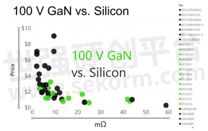
This is the most common myth about GaN technology! GaN devices have been on the market since about 2015 that are lower in price when compared with silicon power MOSFETs with the same on-resistance and voltage ratings. This trend has continued since then as production volumes increased, while at the same time, technology has improved, and die-shrinks have been achieved. The chart below shows a comparison of prices for EPC’s 100 V GaN FETs and their MOSFET counterparts at various on-resistance specifications.

This comparison does not even consider system-level costs. As an example, in a 3 kW 48 V to 12 V DC-DC converter for automotive electric systems, the fast-switching speed of GaN allows a solution that can operate at a higher frequency and higher efficiency enabling a reduction in the number of required phases from a five-phase MOSFET system to a four-phase GaN system that is 35% smaller and lower cost.
Myth #6: GaN technology is not ready for widespread adoption
GaN started commercial production in March of 2010, and lidar was the first ‘killer app’ to use the high speed and tiny size of GaN transistors to maximize performance. This was soon followed by 48V DC-DC converters for high-density computing. Satellite systems began using GaN FETs in volume as they became aware of the excellent properties of GaN in environments that involve multiple forms of radiation. Hundreds of thousands of GaN FETs and hybrid modules have obtained flight heritage everywhere from low Earth orbit to the more stringent geosynchronous Earth orbit. High voltage (650V) GaN FETs and ICs from companies such as Navitas Semiconductor, Power Integrations, and GaN Systems developed the first high-volume consumer market for GaN, the cellphone fast charger. E-bikes, drones, and robots soon adopted GaN to reduce weight, size, cost, and EMI. Automotive applications such as 48 V DC-DC converters, headlamps, cabin fans, seat heaters, and onboard chargers are all moving towards GaN as volumes increase, reliability is proven, and prices decrease.
At this point, GaN is no longer a ‘science project’, but a broad-scale replacement for silicon MOSFETs in applications ranging from 15 V up to 650 V.
Conclusion
Today’s GaN technology is improving rapidly in performance, reliability, and cost and the current benchmark devices are still 100s of times away from their theoretical performance limits. Incumbent MOSFET suppliers, recognizing their products are near their performance limits and a viable competitive solution is gaining acceptance, are using scare tactics to perpetuate myths about GaN.
GaN has emerged as a broad-scale replacement for silicon offering greater efficiency, smaller size, higher reliability, and lower cost. At this point, there are a few reasons not to use GaN FETs and GaN ICs. Learn more about the future of GaN technology, or speak directly with a GaN Expert to get started on your design.
- |
- +1 赞 0
- 收藏
- 评论 0
本文由叫我大表哥吧转载自EPC GaN Talk,原文标题为:Myths about Gallium Nitride Semiconductors,本站所有转载文章系出于传递更多信息之目的,且明确注明来源,不希望被转载的媒体或个人可与我们联系,我们将立即进行删除处理。
相关推荐
【技术】氮化镓场效应晶体管两种散热方式,你知道么?
EPC场效应晶体管的D2PACK封装具的RθJA值小至18℃/W,而封装SO-8具有RθJA值大到34℃/W。
【应用】国产GaN驱动器SGM48520助力激光雷达设计,传播延迟低至2.5ns
激光雷达(LiDAR)属于一种遥感技术,工作原理是通过GaN的高频开关来激发激光二极管实现测距,而驱动GaN FET则需要专门的驱动器,本文介绍国产圣邦微(SGMICRO)的GaN驱动器SGM48520助力激光雷达发射链路中GaN的驱动设计。
EPC(宜普)eGaN® 氮化镓晶体管(GaN FET)和集成电路及开发板/演示板/评估套件选型指南
目录- eGaN FETs and ICs eGaN® Integrated Circuits Half-Bridge Development Boards DrGaN DC-DC Conversion Lidar/Motor Drive AC/DC Conversion
型号- EPC2212,EPC2214,EPC2059,EPC2216,EPC2215,EPC2218,EPC2016C,EPC2050,EPC2052,EPC2051,EPC2054,EPC2053,EPC2055,EPC9086,EPC2218A,EPC90153,EPC9087,EPC90154,EPC2069,EPC2102,EPC2101,EPC2104,EPC2103,EPC2106,EPC2105,EPC2107,EPC9018,EPC2065,EPC90151,EPC21702,EPC90152,EPC2067,EPC2100,EPC2221,EPC21701,EPC2066,EPC90150,EPC90145,EPC9097,EPC90142,EPC9098,EPC90143,EPC9099,EPC90148,EPC9092,EPC90149,EPC90146,EPC9094,EPC90147,EPC2219,EPC9091,EPC2619,EPC2036,EPC2035,EPC2038,EPC2037,EPC2014C,EPC2039,EPC9507,EPC2030,EPC2032,EPC9067,EPC2031,EPC9068,EPC2152,EPC2033,EPC9063,EPC9186,EPC8010,EPC9066,EPC9180,EPC2204A,EPC9181,EPC9061,EPC2308,EPC2307,EPC9005C,UP1966E,EPC2203,EPC9004C,EPC2202,EPC2204,EPC2015C,EPC2207,EPC2206,EPC2040,EPC2045,EPC2044,EPC9194,EPC2012C,EPC2019,EPC9049,EPC9203,EPC9204,EPC9205,EPC2252,EPC9166,EPC9167,EPC9047,EPC9201,EPC9041,EPC9162,EPC9163,EPC9165,EPC7020,EPC9160,EPC9040,EPC90133/,EPC2024,EPC2302,EPC8009,EPC2001C,EPC2029,EPC2304,EPC2306,EPC2305,EPC8002,EPC2021,EPC9177,EPC2020,EPC9057,EPC9167HC,EPC2023,EPC9058,EPC9179,EPC2022,EPC8004,EPC9059,EPC9173,EPC9174,EPC9055,EPC9176,EPC9170,EPC9050,EPC9171,EPC9172,EPC2010C,EPC2034C,EPC7007,EPC7002,EPC9148,EPC2071,EPC7001,EPC23101,EPC23102,EPC23103,EPC90140,EPC9144,EPC23104,EPC2111,EPC7004,EPC2110,EPC7003,EPC90133,EPC90132,EPC9022,EPC9143,EPC90137,EPC90138,EPC90135,EPC90139,EPC7019,EPC7018,EPC9038,EPC9159,EPC2007C,EPC9039,EPC21603,EPC9156,EPC9036,EPC9157,EPC2088,EPC7014,EPC9037,EPC21601,EPC9158,EPC90122,EPC9151,EPC90123,EPC9031,EPC90120,EPC9153,EPC90121,EPC9033,EPC9154,EPC90124,EPC9150,EPC90128
用于DC-DC转换的镓氮®FET和IC应用简介
描述- 本资料介绍了eGaN® FETs和ICs在DC-DC转换中的应用,重点强调了其高效能、高功率密度和小型化的特点。资料中详细展示了不同型号的产品及其在48V至12V转换中的应用,包括高效能计算和电信应用,以及汽车电子领域。此外,还提供了相关产品的详细规格和开发板信息,以帮助工程师进行设计和评估。
型号- EPC2057,N/A,EPC2059,EPC9003C,EPC2215,EPC2218,EPC2016C,EPC2052,EPC2051,EPC2053,EPC2055,EPC90155,EPC90156,EPC90153,EPC2101,EPC2106,EPC2105,EPC90151,EPC2065,EPC90152,EPC2067,EPC2100,EPC9014,EPC2066,EPC90150,EPC9097,EPC90145,EPC90142,EPC9098,EPC90143,EPC9099,EPC9092,EPC90148,EPC90146,EPC90147,EPC9091,EPC2619,EPC2014C,EPC2030,EPC2032,EPC2152,EPC2031,EPC2033,EPC9060,EPC9061,EPC9062,EPC2308,EPC2307,EPC9005C,EPC2204,EPC2207,EPC2206,EPC9195,EPC2019,EPC9166,EPC2252,EPC9047,EPC9162,EPC9041,EPC9163,EPC9165,EPC9160,EPC2302,EPC2304,EPC2306,EPC9010C,EPC2305,EPC9177,EPC2020,EPC9179,EPC2023,EPC9174,EPC9055,EPC9170,EPC9006C,EPC2234,EPC2010C,EPC9148,EPC23101,EPC2071,EPC23102,EPC23103,EPC23104,EPC90140,EPC9143,EPC90132,EPC90137,EPC91106,EPC90138,EPC90135,EPC91108,EPC9159,EPC2007C,EPC2361,EPC9157,EPC9036,EPC9158,EPC9037,EPC2088,EPC9151,EPC90122,EPC9031,EPC90123,EPC9153,EPC90120,EPC9033,EPC90124
EPC eGaN®FET/晶体管选型表
EPC提供增强型氮化镓半桥功率晶体管/增强型功率晶体管/功率晶体管的选型:配置:Dual Common Source、Dual with Sync Boot、Half Bridge、Half Bridge Driver IC、HS FET + Driver + Level Shift、Single、Single - AEC Q101、Single – Rad Hard、Single with Gate Diode、Single with Gate Diode – AEC-Q101、Dual Common Source - AEC Q101,VDS最大值(V):15~350V;VGS最大值(V):5.75~7V
|
产品型号
|
品类
|
Configuration
|
VDSmax(V)
|
VGSmax(V)
|
Max RDS(on) (mΩ)
@ 5 VGS
|
QG typ(nC)
|
QGS typ (nC)
|
QGD typ (nC)
|
QOSS typ (nC)
|
QRR(nC)
|
CISS (pF)
|
COSS (pF)
|
CRSS (pF)
|
ID(A)
|
Pulsed ID (A)
|
Max TJ (°C)
|
Package(mm)
|
Launch Date
|
|
EPC2040
|
Enhancement Mode Power Transistor
|
Single
|
15
|
6
|
30
|
0.745
|
0.23
|
0.14
|
0.42
|
0
|
86
|
67
|
20
|
3.4
|
28
|
150
|
BGA 0.85 x 1.2
|
Apr, 2017
|
选型表 - EPC 立即选型
【IC】EPC提供100V GaN FET助力实现更小的电机驱动器,用于电动自行车、机器人和无人机
EPC推出三相BLDC电机驱动逆变器参考设计EPC9194,工作输入电源电压范围为14V~60V,可提供高达60Apk的输出电流。此电压范围和功率使该解决方案非常适合用于各种三相BLDC电机驱动器,包括电动自行车、电动滑板车、无人机、机器人和直流伺服电机。
氮化镓集成电路简化仿人机器人电机关节逆变器设计
描述- 本文介绍了基于氮化镓(GaN)技术的逆变器设计,特别是在人形机器人电机关节逆变器中的应用。文章强调了GaN技术在提高开关频率、降低无源元件数量、减少开关损耗和提高功率密度方面的优势。EPC ePower™ Stage ICs技术简化了逆变器设计,并介绍了EPC23102/3/4系列GaN集成电路及其在逆变器性能中的应用。文章还讨论了EPC提供的参考设计板,这些设计板展示了GaN技术在电机驱动逆变器设计中的简化与空间减少。实验结果表明,GaN技术的应用提高了系统效率,并实现了更紧凑的逆变器设计。
型号- EPC2310X,EPC9186,EPC9176,EPC91104,EPC9194,EPC23102,EPC23103,EPC23104,EPC9176V3
EPC GaN FET助力DC/DC转换器实现功率密度和效率基准
EPC GaN FET与Analog Devices驱动器和控制器相结合,为客户简化氮化镓基设计、提高其效率、降低散热成本、助力计算、工业和消费类应用的DC/DC转换器实现最高功率密度。
【元件】EPC推出首款具有最低1mΩ导通电阻的GaN FET EPC2361,采用紧凑型QFN封装(3mmx5mm)
EPC推出采用紧凑型QFN封装(3mmx5mm)的100V、1mOhm GaN FET(EPC2361),助力DC/DC转换、快充、电机驱动和太阳能MPPT等应用实现更高的功率密度。
氮化镓可靠性和寿命预测:第16阶段
描述- 本报告详细探讨了氮化镓(GaN)器件的可靠性,包括失效机制、测试方法以及在不同应用中的可靠性预测。报告重点介绍了测试至失效方法在确定GaN器件内在失效机制方面的作用,并提供了针对不同应用(如太阳能、DC-DC转换和激光雷达)的可靠性预测指南。此外,报告还讨论了热机械可靠性、过电压指南以及优化焊接工艺的方法。
型号- EPC2302,EPC2218A,EPC23102,EPC21701,EPC21601
【元件】使用EPC新款50V GaN FET设计更高功率密度的USB-C PD应用,尺寸仅为1.8 mm²
EPC推出了50V、8.5mOhm的EPC2057 GaN FET,尺寸仅为1.5mm x 1.2mm,为USB-C PD应用提供了更高的功率密度。加利福尼亚州埃尔塞贡多—2024年6月—EPC是增强型氮化镓(GaN) 功率FET和IC的全球领导者,推出了50V、8.5mΩ的EPC2057。该GaN FET专为满足高功率USB-C设备的不断发展需求而设计,包括消费电子、车载充电和电动出行设备。
【经验】GaN FET在激光雷达驱动器中的参数设计指导
本文中给出的激光雷达驱动器采用EPC公司的开发板EPC9126进行设计。EPC9126/EPC9126HC采用最优的PCB layout,EPC9126采用GaN FET—EPC2016C,在极短的4ns脉冲宽度,给三接面激光产生35A脉冲。EPC9126HC为大电流演示系统,在 8ns脉冲宽度可产生65A脉冲。文中给出了具体设计的参数指导。
SC8901 5V 7A/5A 低侧 GaN 和 MOSFET 驱动器
描述- SC8901是一款低侧GaN和MOSFET驱动器,具有超快传播延迟和最小脉冲宽度,适用于激光雷达、飞行时间激光驱动器、面部识别等应用。产品采用WLCSP-6B封装,提供UVLO和OTP保护功能。
型号- SC8901KFLUMY,SC8901
【视频】EPC氮化镓产品在DCDC的应用,可减少损耗
描述- Efficient Power Conversion (EPC) 作为全球领先的功率转换技术供应商,提供基于氮化镓 (GaN) 的场效应晶体管 (FET) 和集成电路 (IC)。EPC 的 GaN 基器件具有高效率、快速开关速度、小型化和低成本等优势,广泛应用于消费电子、通信、汽车和可再生能源领域。资料中详细介绍了 GaN 基 DC-DC 转换器,包括企业电源架构、功率密度、EPC9159 转换器规格、转换器概述、特色 GaN FET 以及效率与损耗测量等。此外,还讨论了 GaN FET 在提高功率密度和简化设计方面的优势。
型号- EPC2302,EPC2305,EPC2308,EPC23101,EPC23102
【IC】EPC新推基于GaN FET的150A电机驱动器EPC9186,适用于电动出行、叉车和大功率无人机
EPC新推EPC9186,这是一款采用EPC2302 eGaN®FET的三相BLDC电机驱动逆变器。EPC9186支持14V~80V的宽输入直流电压。大功率EPC9186支持电动滑板车、小型电动汽车、农业机械、叉车和大功率无人机等应用。
电子商城
现货市场
服务
满足150W内适配器、PD快充、氮化镓快充等主流产品测试需要;并可查看被测开关电源支持协议,诱导多种充电协议输出,结合电子负载和示波器进行高精度测试。测试浪涌电流最大40A。支持到场/视频直播测试,资深专家全程指导。
实验室地址: 深圳 提交需求>
支持GSM / GPRS 等多种制式产品的射频测试,覆盖所有上行和下行的各项射频指标,包括频差、相差、调制、功率、功控、包络、邻道泄漏比、频谱、杂散、灵敏度、同道干扰、邻道干扰、互调、阻塞等等。满足CE / FCC / IC / TELEC等主流认证的射频测试需求。
实验室地址: 深圳 提交需求>


登录 | 立即注册
提交评论