How to Design a 12V-to-60V Boost Converter with Low Temperature Rise Using eGaN FETs


Modern displays, such as laptops and PC monitors, typically require a low power boost converter. In this application, the screen intensity is low to moderate and the converter is operated at light load most of the time, so the light-load efficiency is very important. The low switching loss of eGaN FETs can help address this challenge. This GaN Talk will examine the design of a 12V to 60V, 50W DC/DC power module with low temperature rise using eGaN FETs in the simple and low-cost synchronous boost topology.

Design of a small and Highly Efficient eGaN®-FET-based synchronous boost converter
The synchronous boost topology is popular in DC/DC step-down converter design for its simplicity, easiness in control, and low cost. The schematic diagram of the eGaN FET-based synchronous boost converter is shown in Figure 1. The 100V rated eGaN FET EPC2052 with RDSon of 6mΩ is selected for the 12V to 60V, 50W power stage. The uP1966E gate driver that features high driving strength is used to drive the FETs. The synchronous bootstrap circuit with EPC2038 that ensures 4.9V gate voltage is used for the high-side gate drive. Digital control that allows sub-10ns dead time and flexibility in control scheme development is employed. To optimize efficiency, two small on-board switch-mode power supply circuits are used to generate the housekeeping 5V and 3.1V voltages for the gate driver and the digital controller respectively. The house keeping power can also be powered from either high or low voltage port using the simple diode“OR”circuit, which enables bi-directional operation.

Figure 1. Simplified schematic of the eGaN FET-based synchronous boost converter. The design is bi-directional capable.
The switching frequency of the converter is designed at 500kHz for high light-load efficiencies, and the inductor is a 10μH TDK ferrite inductor. At light load, the inductor core and AC copper losses are dominating factors. Therefore, a larger inductor improves the light-load efficiency because of decreased ripple and thus lower core losses and AC copper losses.
Design Validation
The synchronous boost converter EPC9162 is shown in Figure 2. The switch-node voltage, VSW waveform at 0.15A output current is presented in Figure 3, which shows the switching to be fast and clean.
The overall power efficiency and power loss of the synchronous boost converter operating at different input voltages are given in Figure 4 with a peak efficiency of 95.3% at 12V input and 60V and 0.85A output.

Figure 2. Photograph of the 1 V to 60V, 50W synchronous boost converter EPC9162
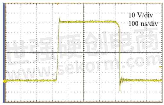
Figure 3. Switch-node voltage vSW, waveform at 0.15A output current
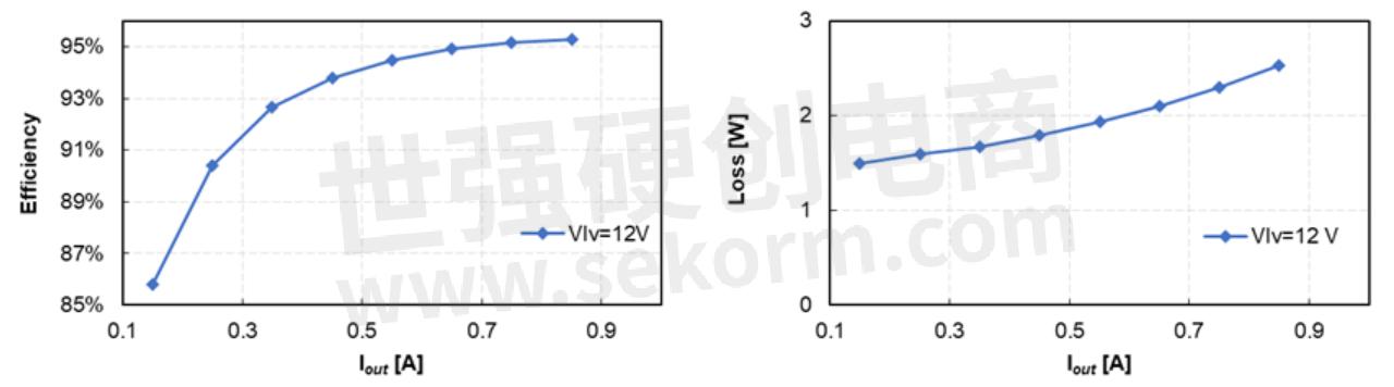
Figure 4. Total system efficiency, including the housekeeping power consumption at 20V output
The thermal image of the converter operating at 12V to 60V, 0.85A output current without forced-air cooling is shown in Figure 5. A temperature rise of just 40°C is achieved. It is clear that the GaN FETs are capable of carrying more current given a relaxed temperature rise or with forced-air cooling.
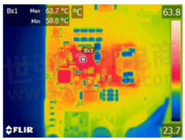
Figure 5. Thermal image of the synchronous boost converter operating at 12V to 60V and 0.85A output and thermal steady state without forced-air cooling
Conclusions
A 12V to 60V, 50W eGaN-FET-based synchronous boost converter achieves 95.3% peak efficiency and only 40°C temperature rise with the small die size of 2.25mm2. In applications where light-load efficiency is critical such as LED backlighting for laptops and monitors, the fast switching speed of eGaN FETs significantly reduces switching losses for higher efficiency. Additionally, the low temperature rise prevents equipment overheating and the synchronous boost topology provides a simple, low-cost solution.
- |
- +1 赞 0
- 收藏
- 评论 0
本文由董慧转载自EPC,原文标题为:How to Design a 12V-to-60V Boost Converter with Low Temperature Rise Using eGaN FETs,本站所有转载文章系出于传递更多信息之目的,且明确注明来源,不希望被转载的媒体或个人可与我们联系,我们将立即进行删除处理。
相关推荐

【经验】EPC eGaN FET和eGaN IC PCB封装设计指南
一个良好的PCB封装设计对于GaN器件的一致性和可靠性是很重要的。本文是根据数据手册为EPC器件设计正确封装的指导原则——以EPC2016C和EPC2045为例,分别从LGA和BGA封装来完成介绍。

【经验】与前代eGaN FET保持“相容”同时,宜普第二代增强型无铅eGaN®FET提供更优异性能
无铅eGaN FET中EPC2XXX系列技术资料,帮助工程師利用宜普产品设计最优异性能产品或解決方案,产品系列包括EPC2001、EPC2007、EPC2015、EPC2014、EPC2010及EPC2012。

【经验】EPC分享eGaN FET如何缩小现代电源电路的物理尺寸——以LLC谐振转换器的设计为例
EPC设计的氮化镓场效应管具有小尺寸,高功率密度的特点,本文从LLC谐振转换器的设计说明了eGaN FET如何缩小现代电源电路的物理尺寸,并提高功率密度。

EPC eGaN®FET/晶体管选型表
EPC提供增强型氮化镓半桥功率晶体管/增强型功率晶体管/功率晶体管的选型:配置:Dual Common Source、Dual with Sync Boot、Half Bridge、Half Bridge Driver IC、HS FET + Driver + Level Shift、Single、Single - AEC Q101、Single – Rad Hard、Single with Gate Diode、Single with Gate Diode – AEC-Q101、Dual Common Source - AEC Q101,VDS最大值(V):15~350V;VGS最大值(V):5.75~7V
|
产品型号
|
品类
|
Configuration
|
VDSmax(V)
|
VGSmax(V)
|
Max RDS(on) (mΩ)
@ 5 VGS
|
QG typ(nC)
|
QGS typ (nC)
|
QGD typ (nC)
|
QOSS typ (nC)
|
QRR(nC)
|
CISS (pF)
|
COSS (pF)
|
CRSS (pF)
|
ID(A)
|
Pulsed ID (A)
|
Max TJ (°C)
|
Package(mm)
|
Launch Date
|
|
EPC2040
|
Enhancement Mode Power Transistor
|
Single
|
15
|
6
|
30
|
0.745
|
0.23
|
0.14
|
0.42
|
0
|
86
|
67
|
20
|
3.4
|
28
|
150
|
BGA 0.85 x 1.2
|
Apr, 2017
|
选型表 - EPC 立即选型

【应用】eGaN FET EPC2051助力激光雷达发射端高功率纳秒级别脉冲设计
在激光雷达的发射链路中,为实现雷达高分辨率的设计,需产生高功率、纳秒级别的激光脉冲。要达到这样的设计要求,普通MOS不能满足要求,需要采用GaN 搭配高功率Laser器件进行实现。EPC2051是EPC公司生产的氮化镓场效应晶体管(eGaN FET),已经成功的应用在激光雷达上。

EPC2057氮化镓场效应晶体管材料成分声明
本资料为EPC2057元器件的材料成分声明,由Efficient Power Conversion (EPC)公司于2024年7月8日发布。声明中详细列出了该元器件的各组成部分及其所含物质,包括硅、氧化硅、氮化硅、氮化镓、铝、氮化铝、钛、氮化钛、铜、钨、聚酰亚胺等,并提供了每种物质的CAS编号、重量百分比和总重量。声明强调,所提供的数据为估算值,可能因技术要求和开发而变化,EPC可能随时更新此文件,且声明可能不包括最终产品中电气设备内掺杂剂和金属材料的微量信息。
EPC - EGAN FET,氮化镓场效应晶体管,EPC2057

【应用】eGaN FET EPC2007C成功助力16线、32线等多线激光雷达发射端纳秒级别脉冲设计
在激光雷达的发射链路中,为实现雷达高分辨率的设计,需产生高功率、纳秒级别的激光脉冲。要达到这样的设计要求,需要采用GaN搭配高功率Laser器件来实现。EPC2007C为EPC的氮化镓场效应晶体管(eGaN FET),已经成功的应用在16线、32线等激光雷达设计上。

【产品】EPC新型200V eGaN FET的性能相比传统Si MOSFET提高了一倍
EPC推出新型200V eGaN FETs(氮化镓增强型功率晶体管),相比于传统的硅功率MOSFET的性能提高了一倍。新第五代设备的尺寸仅为上一代产品的一半,栅电极和源电极之间的距离有所减小,金属层的厚度增加等诸多改进使第五代FET的性能提高了一倍。
EPC2934C氮化镓场效应晶体管材料成分声明
本资料为EPC2934C元器件的材料成分声明,由Efficient Power Conversion (EPC)公司于2024年5月6日发布。声明中详细列出了该元器件的各组成部分及其所含物质,包括硅、氮化镓、铝、钛、铜、钨、聚酰亚胺等,并提供了每种物质的CAS编号、重量百分比和总重量。声明强调,所提供的数据为估算值,可能因技术要求和开发而变化,EPC可能随时更新此文件,且声明可能不包括最终产品中电气设备内掺杂剂和金属材料的微量信息。
EPC - EGAN FET,氮化镓场效应晶体管,EPC2934C

BRC Solar Selects EPC 100V eGaN FETs for Next Generation Solar Optimizer
Designing EPC‘s EPC2218 100V FETs into BRC Solar GmbH‘s next generation M500/14 power optimizer has enabled a higher current density due to the low power dissipation and the small size of the GaN FET making the critical load circuit more compact.
EPC 29215_55氮化镓场效应晶体管材料成分声明
本资料为EPC29215\_55型号元器件的材料成分声明。声明中详细列出了芯片的构成元素、相应物质、CAS编号、重量百分比和总重量。声明指出,所提供的数据为近似值,基于工程计算,可能因技术要求和开发而随时更改。EPC可能不通知即更新此文件。声明可能不包括最终产品中电气设备内掺杂剂和金属材料的微量信息。
EPC - EGAN FET,氮化镓场效应晶体管,EPC29215_55

EPC Launches 40V EPC2055 eGaN FET Ideal for High Power Density Solutions for USB-C Battery Chargers and Ultra-thin Point-of-Load Converters
December 2020 — Efficient Power Conversion (EPC) Corporation advances the performance capability of low voltage, off-the-shelf gallium nitride transistors with the introduction of the EPC2055 (3mΩ, 40V) eGaN FET. This device is ideal for applications with demanding requirements for performance in space-constrained form factors including USB-C batter chargers and ultra-thin point-of-load (POL) converters.
EPC评估套件选型表
EPC提供评估板的选型:Default Configuration:IToF、Resonant Pulse DToF;VBUS (max)(V):12~160V;VINPUT(max)(V):5 V;Tpin(min)(ns):1 ns/2 ns
|
产品型号
|
品类
|
Description
|
VIN(V)
|
VOUT(V)
|
IOUT (A)
|
Featured Product
|
|
EPC9163
|
评估板
|
Synchronous, Buck or Boost, digital controller
|
Buck: 20 – 60 V
Boost: 11.3 – 16 V
|
Buck: 5 - 16 V
Boost: 20-50 V
|
140 A (Buck)
|
EPC2218
|
选型表 - EPC 立即选型
EPC2215氮化镓场效应晶体管材料成分声明
本资料为EPC2215元器件的材料成分声明,由Efficient Power Conversion (EPC)公司于2024年4月24日发布。声明中详细列出了该元器件的各个构造元素及其对应的物质、CAS编号、重量百分比和总重量百分比。声明中提到的物质包括硅、氧化硅、氮化硅、氮化镓、铝、氮化铝、钛、氮化钛、铜、钨、聚酰亚胺、钛金属、镍、锡和银等。声明强调,所提供的数据为近似值,基于工程计算,可能因技术要求和开发而随时更改,EPC可能不另行通知更新此文件。声明可能不包括关于最终产品中包含的电气设备中掺杂剂和金属材料的微量信息。
EPC - EGAN FET,氮化镓场效应晶体管,EPC2215

【产品】全新170V/6.8mΩ的eGaN FET EPC2059,尺寸仅2.8×1.4mm
EPC推出的EPC2059是一款增强型氮化镓功率晶体管(eGaN FET),漏源电压170V,典型导通电阻6.8mΩ,连续漏极电流24A,脉冲漏极电流102A,仅以带有焊条的钝化芯片形式提供,芯片尺寸2.8mm×1.4mm,无卤素。

电子商城


授权代理品牌:集成电路


授权代理品牌:分立元件


授权代理品牌:接插件及结构件


授权代理品牌:部件、组件及配件


授权代理品牌:电源及模块


授权代理品牌:电子材料


授权代理品牌:仪器仪表及测试配组件


授权代理品牌:电工工具及材料


授权代理品牌:机械电子元件


授权代理品牌:加工与定制


登录 | 立即注册
提交评论