SanDeYing Electronic PCB 3D Models Provides A Clear View of All The Parts on PCB Boards in 3 Dimensions Length, Width, and Height




The 3D model provides a clear view of all the parts on PCB boards in 3 dimensions length, width, and height. So that it helps to select suitable-sized parts, optimize the layout and fit the PCB inside an enclosure.
The PCB panel allows you to browse the current PCB design using a range of filter modes to determine which object types or design elements are listed, highlighted, or selected. The panel also has editing modes for specific object types or design elements that provide dedicated controls for editing procedures. Note that you can access the properties for any element listed in the panel.
The three main list regions of the panel when in 3D Model mode reflect, in order from the top:
1. Component classes.
2. Specific components associated with the component class that has associated 3D body object(s) or free models (non-PCB mounted, free-floating 3D bodies).
3. The individual 3D bodies for each component or free model.
Panel Access
When the PCB Editor is active, click the PCB button at the bottom-right corner of the workspace and select PCB from the context menu. Alternatively, you can access the panel through the View » Workspace Panels » PCB » PCB sub-menu.
Panels can be configured to be floating in the editor space or docked to the sides of the screen. If the PCB panel is currently in a group of panels, use the PCB tab located at the bottom of the panels to bring it to the front.
Browsing 3D models
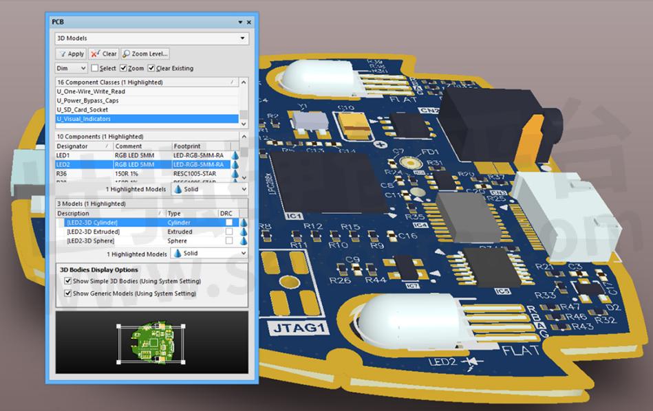
The PCB panel's filter scope progresses through component classes to components and their constituent model elements, while the visual result tracks the changes.
As you click on a specific component in the Components region of the panel, filtering will be applied using the component as the scope of the filter. The visual result (in the design editor window) is determined by the highlighting methods enabled (Mask/Dim/Normal, Select, Zoom). Multiple rule entries can be selected using standard Shift+Click and Ctrl+Click features.
Double-clicking a component entry in the Component region of the panel (or right-clicking and choosing Properties) will open the relevant Component dialog, from which you can edit its properties in detail.
Similarly, double-clicking a model entry in the Models region of the panel (or right-clicking and choosing Properties) will open the relevant 3D Body dialog, from where you can edit the complete 3D body properties.
When selecting a component's constituent models from the Models list area in the PCB panel, the view in the editor workspace will zoom, dim/mask, or select accordingly.
An individual model is selected from a component. In this case, a cylinder from a LED component in the board's U_Visual_Indicators class.
The PCB panel can be used to select display properties for 3D models. The cone icons represent different levels of transparency from 100% (hidden) down to 0% (solid) in increments of 25%. You can select multiple components and apply the same display controls to them at once using the Highlighted Models options.
The selected cylinder model is set to 75% opacity. Multiple models can also be selected and changed in one step.
Enable the DRC checkboxes for models you want to be flagged for analysis under the Placement » Component Clearance rule.
The 3D Bodies Display Options controls allow you to control the display of 3D bodies without having to modify the current view configuration. Display options set from the PCB panel are not saved as part of the view configuration.
Multiple Model entries can be selected using standard Shift+Click and Ctrl+Click features, providing full control over the 3D Model view and the base 3D elements that make up a component.
Here, both a cylinder (set to 75% opacity) and a sphere (solid / 0% opacity) from a LED component are selected.
3D Body Display Options
Show Simple 3D Bodies (Using System Setting) - Enable this option to display simple 3D bodies on the PCB. This option is enabled by default.
Show Generic Models (Using System Setting) - Enable this option to display generic models on the PCB. This option is enabled by default.
- |
- +1 赞 0
- 收藏
- 评论 0
本文由PlusLee转载自SDY News,原文标题为:三德盈 Electronic PCB 3D models,本站所有转载文章系出于传递更多信息之目的,且明确注明来源,不希望被转载的媒体或个人可与我们联系,我们将立即进行删除处理。
相关推荐
Selection of Fuses in Small Home Appliance PCB Board
The fuses commonly used in PCB boards of small household appliances use self-recovery fuses to protect the circuit.
Explaining the Thermal Design and Management
Overheating (temperature rise) has always been the enemy of stable and reliable product operation,Here DIANYANG is mainly to talk about Thermal design and management.
How to Debug a Newly Developed Circuit Board?
For a newly designed circuit board, it is often difficult to debug it, especially when the board is relatively large and there are many components, it is often impossible to start. How to debug a newly developed circuit board? SIFU will explore in this article.
4 Key Factors on Copper Plating
There are four key factors on copper plating process to ensure good quality of copper inside holes:Board abrasion,Board cleaning,Desmear and The copper plating facility.
Types of PCB Board Surface Finishes
The surface finish is a very important consideration that impacts PCB assembly and your board’s reliability by protecting copper traces and strengthening solder connections.
One of The Most Widely Used Pcb Layout Software:Altium Designer Preferences Setting
Altium Designer is one of the most widely used PCB layout software. It is popular among PCB board designers due to some features, like schematic capture, 3D PCB design, FPGA development, and release/data management.
Managing the Impact of PCB Material Properties on Your Board‘s Manufacture
The PCB material properties will determine how your PCB will function as well as your board’s quality and reliability. Therefore, it is necessary to define them during design so they can be incorporated into the PCB manufacturing process.
Suggestions on the Design of PCB Laminated Structure
Here are some suggestions on the design of the PCB laminated structure. In a small number of PCB designs, we use the power supply ground plane wiring or the power grid and the ground network in the wiring layer. For this hybrid type of level design, we call it the signal level.
What Is the Design Standard of PCB Pad?
When designing PCB soldering plates in the design of PCB, it is necessary to design strictly according to the relevant requirements. Because in the process of SMT patch, the design of the PCB pad is very important. The design of the pad will directly affect the weldability, stability, and heat transfer of components.
Do You Know the Factors that Lead to the Loss of the PCB circuit board?
Moisture is the most common and most destructive factor for the PCB circuit board. Excessive moisture can greatly reduce the insulation resistance between the conductors, accelerate the high-speed decomposition, reduce the Q value, and corrode the conductor.
IS6630A/C/D with Three-way Output Enables DDR Power Supply Integration, Saving the Space on the PCB Board And the Required Devices
As a fully integrated DDR power supply integrated power supply solution, IS6630A / C / D is mainly used in high data transmission rate / wide output voltage range of pen, data center and other industries, taking into account high efficiency, high performance, while having a smaller application volume, can match the mainstream market demand, and actively enable the development of DDR industry.
Bornsun Offers Many Thermal Interface Thermal Conductive Materials that Can be Applied to UPS
UPS is an uninterruptible power supply containing energy storage devices, rectifiers, inverters, batteries as the main components, mainly for the power supply stability requirements of higher equipment to provide uninterruptible power supply. This article introduces Bornsun‘s thermal interface thermal conductive materials that can be applied to UPS.
RF Chip Testing Socket Automatically Matched BGA Solder Balls, Ensuring High Reliability Performance
Flip over BGA sockets do not require installation tools or mounting holes on the target PCB board, maximizing space savings while reducing board costs; This product provides a compact surface mount testing solution using a small pitch micro BGA testing, debugging, and verification chipset; The compact device with surface mount design provides precision machined spring probes and automatically matched BGA solder balls, ensuring high reliability performance.
MOS Tube Knowledge, Must Read!
According to the size of PCB board, select the appropriate PMOS tube size, in the case of limited on-board area, choose the small package as far as possible; As far as possible to select common packaging, to prepare for the subsequent selection of appropriate replacement material.
维峰电子(WCON)机加工排母排针连接器选型指南
Maching Pin Header Flexible Install To PCB Board Maching Female Header Flexible Install To PCB Board 1.27mm Machined Female/Pin Header Connector 1.27*2.54mm Machined Female/Pin Header Connector 1.778mm Machined Pin/Female Header Connector 2.00mm Machined Female/Pin Header Connector 2.54mm Machined Female/Pin Header Connector 1.778mm IC Socket Connector and Adapter 2.54mm IC Socket Connector 2.54mm Maching Pin Adapter Connector Machined Female Terminal Machined Male Pins Terminal
维峰电子 - MACHING FEMALE HEADER,IC SOCKET CONNECTOR,机加工销头连接器,IC插座连接器,机加工母端子,加工排针,MACHINED FEMALE TERMINAL,MACHING PIN HEADER,ADAPTER,机加工插脚端子,MACHING PIN ADAPTER CONNECTOR,加工插针适配器连接器,MACHINED FEMALE HEADER CONNECTOR,适配器,FEMALE HEADER,机加工排母连接器,MACHINED PIN HEADER CONNECTOR,MACHINED MALE PINS TERMINAL,机加工排母,IC SOCKET ADAPTER,PIN HEADER,3510-302XXSGX100X1,3510-302XXSGX146X1,T3520-054-24XXBXX01,10-30564SXXXXXX1,3520-302XXSSXXXXX1,3511-301XXMGX112T1,3560-30550SGXXXXXX,7110-30242RXX097X1,7110-19124SXX048X1,3514-192XXSGX081X1,3521-852XXSSX115T1,7110-30228SSX074X1,3524-XXXXXRSX089X1,7120-30228SXX074X1,7110-30320SSX074X1,7110-30324SXXXXXX1,7110-30118RXX097X1,3560-30332SGXXXXXX,3511-30XXXXGX112XX,7110-30324MXX042X1,7110-30332MXX074X1,7110-19236SXX048X1,3515-192XXSGX081T1,3561-30XXXSGX100T1,7110-30248SXX178X1,3521-421XXSSX074T1,3521-70XXXXSXXXXXX,3520-301XXRSX097X1,3561-30242SXX100X1,3512-281XXRGX121X1,3520-301XXSSX054X1,7110-30328SXX178X1,3524-382XXMSX060T1,7110-30114MXX074X1,3560-30120MXX102X1,7110-30122SXX178X1,7110-30128MXX074X1,T3520-0743-28XXBXX01,7110-30322RXX097X1,3560-301XXSXX122X1,3560-30114SGXXXXXX,7110-30106SXXXXXX1,7120-30464SXX074X1,3560-30128SGXXXXXX,T3520-074-32XXBXX01,3520-30XXXSSX142X1,T3524-060-24XXBXX01,3510-302XXSGX124X1,T3522-094-32XXBXX01,7110-30240SSX074X1,3510-302XXSGX122T1,3560-30XXXSXX100X1,3560-30232MXX102X1,7110-30124SXXXXXX1,3521-701XXMSX104XX,3560-30XXXSXX100X2,3522-28XXXSSX074XX,3520-192XXSSX048X1,3525-382XXRSX089X1,3510-301XXSGX215T1,7110-30224RXX097X1,3520-302XXSSX103X1,3521-702XXRSX124X1,7110-19110SXX048X1,7110-30106MXX042X1,7110-30328MXX074X1,3560-30564SGXXXXXX,3520-302XXMSX042T1,3512-282XXMGX100T1,3521-423XXSSX074T1,3510-301XXSGX119X1,7110-30128SXX178X1,3511-302XXSGX112T1,3520-30XXXSSX132X1,3510-30XXXXGX100XX,7110-30252SXX178X1,3512-281XXSGX100T1,3560-303XXSXX122X1,7110-30124MXX042X1,7110-30232SSX074X1,3524-382XXRSX089X1,3561-30248SXX100X1,7110-30XXXSSX178T1,3560-30328SGXXXXXX,3524-383XXSSX060X1,7110-30564SXX178X1,3522-282XXSSX074T1,3522-282XXRSX096X1,7120-30240SXX074X1,7110-30248RXX097X1,3561-30224SXX100X1,3510-192XXSGX076T1,3560-30252SGXXXXXX,3510-301XXRGX127X1,3560-30228MXX102X1,3510-301XXSGX336T1,3520-302XXSSXXXXT1,3511-691XXSGX098X1,3510-302XXSGX146T1,7110-30XXXMSX074T1,3560-30XXXSXX122X1,7110-30122MXX074X1,7110-19240SXX048X1,7110-30114MXX042X1,3514-192XXSGX081T1,3521-702XXSSX100T1,3510-302XXSGX274T1,T3522-096-54XXBXX01,3514-221XXMGX081XX,T3510-137-41-30XXB1,7110-30114SXX178X1,3560-30240MXX102X1,3520-30XXXSSX152X1,3510-302XXSGX100T1,7110-30236SXXXXXX1,3514-XXXXXXGXXXXXX,3510-302XXSGX137X1,7110-30328RXX097X1,3510-30XXXMGX071X1,3522-281XXSSX059T1,7110-30552SSX074X1,3515-192XXSGX081X1,3521-421XXSSX074X1,T3521-100-30XXBXX01,3520-302XXSSX178T1,3521-852XXSSX115X1,3561-30256SXX100X1,3511-301XXRGX136T1,3560-30XXXSGXXXXTX,3514-211XXRGX103X1,7110-30108SSX074X1,3510-301XXMGX100T2,3510-30XXXRGX127X1,7110-30XXXRSX097T1,3510-301XXMGX100T1,7110-30248MXX074X1,3561-30328SXX100X1,7110-30332MXX042X1,7110-19106SXX048X1,3510-302XXSGX124T1,7110-19120SSX048T1,3512-282XXMGX100X1,7110-192XXSSX048T1,3510-301XXSGX215X1,7110-30106MXX074X1,3560-30322SGXXXXXX,7110-302XXMSX074T1,7110-30240SXXXXXX1,T3510-336-30-32XXB1,T3510-274-30-32XXB1,3523-301XXSS074X1,3560-305XXSXX122X1,7110-303XXSSX074T1,7110-30118MXX074X1,3520-301XXSSX074T1,7110-30112RXX097X1,3560-30116MXX102X1,7110-30322SXX178X1,3522-282XXSSX074X1,3520-30XXXRSX097X1,3561-30332SXX100X1,7110-30328MXX042X1,7110-30124SSX074X1,7110-30110SXXXXXX1,3510-301XXSGX336X1,7110-301XXRSX097T1,3510-192XXSGX076X1,7110-30320SXXXXXX1,7110-19120SXX048X1,7110-30116MXX042X1,7110-30124MXX074X1,3510-302XXSGX274X1,3522-282XXMSX074X1,3521-701XXSSX110T1,3511-691XXSGX098T1,3560-30124SGXXXXXX,3521-701XXSSX100X1,3560-30242SGXXXXXX,3510-302XXMGX071X1,7110-30242MXX074X1,3560-303XXMXX102X1,3561-30264SXX100X1,3514-192XXRGX103X1,3510-192XXSGX085T1,3510-191XXSGX076X1,3511-302XXRGX136X1,3560-30224SGXXXXXX,3560-30118SGXXXXXX,7110-19114SXX048X1,3510-302XXSGX137T1,3560-302XXMXX102X1,7110-30320MXX042X1,3522-281XXSSX059X1,3521-702XXSSX100X1,3511-691XXMGX098T1,7110-19232SXX048X1,3520-302XXSSX178X1,3520-301XXSSX143T1,3521-702XXSSX110T1,3560-30236SGXXXXXX,7110-30110MXX074X1,7110-30550SXXXXXX1,3524-383XXRSX089T1,3514-211XXRGX103T1,3511-693XXSGX098T1,T3521-104-34XXBXX01,3560-30110MXX102X1,3560-30324SGXXXXXX,7110-30228RXX097X1,3520-302XXMSX074X1,3524-411XXSSX060X1,7110-30120SXXXXXX1,3514-221XXZGX103X1,3521-702XXSSX110X1,3561-30464SXX100X1,7110-19108SXX048X1,7110-30332SXXXXXX1,3510-301XXSGX274X1,7110-30228MXX042X1,7110-30108SXX178X1,3520-302XXSSX143T1,3520-301XXSSX178T1,3514-XXXXXRGX103X1,3561-30228SXX100X1,3511-692XXSGX098X1,7110-30110SSX074X1,3521-85XXXSSX115X1,3510-302XXSGX215X1,3511-692XXMGX098T1,3510-301XXMGX071X1,7110-303XXMSX074T1,3510-191XXSGX085T1,3515-192XXRGX103X1,3520-30XXXSSX162X1,3522-282XXMSX074T1,7110-30332SXX178X1,T3510-215-30-32XXB1,7110-30108SXXXXXX1,3560-30248SGXXXXXX,3514-192XXRGX103T1,T3514-081-30-30XXB1,3560-30552SGXXXXXX,T3520-103-33XXBXX01,3510-191XXSGX085X1,3514-192XXMGX081T1,7120-30264SXX074X1,3510-302XXMGX071T1,7110-30122RXX097X1,3511-59XXXXGXXXXX1,3511-302XXRGX136T1,3510-302XXRGX127T1,7110-30116RXX097X1,7110-30110MXX042X1,7110-30240RXX097X1,7110-30114SXXXXXX1,3510-192XXSGX085X1,3520-301XXSSX054T1,7110-30110SXX178X1,7110-303XXRSX097T1,7110-30116MXX074X1,3520-301XXRSX097T1,7110-305XXSSX074T1,7110-30128
服务
可定制UV胶的粘度范围:150~25000cps,粘接材料:金属,塑料PCB,玻璃,陶瓷等;固化方式:UV固化;双固化,产品通过ISO9001:2008及ISO14000等认证。
最小起订量: 1支 提交需求>
可定制插座连接器的间距1.25mm~2.54mm;列数:单列/双列/三列/四列;端子类型:直焊针、直角焊针、表面贴装式、无焊柔性针压接、绕接、载体.;镀层、车针长度/直径、连接针长度等参数可按需定制。
最小起订量: 1 提交需求>





登录 | 立即注册
提交评论